ZHCSOS3F August 2021 – March 2024 TPS7H2211-SEP , TPS7H2211-SP
PRODUCTION DATA
- 1
- 1 特性
- 2 应用
- 3 说明
- 4 Device Options
- 5 Related Products
- 6 Pin Configuration and Functions
-
7 Specifications
- 7.1 Absolute Maximum Ratings
- 7.2 ESD Ratings
- 7.3 Recommended Operating Conditions
- 7.4 Thermal Information
- 7.5 Electrical Characteristics: All Devices
- 7.6 Electrical Characteristics: CFP and KGD Options
- 7.7 Electrical Characteristics: HTSSOP Option
- 7.8 Switching Characteristics: All Devices
- 7.9 Quality Conformance Inspection
- 7.10 Typical Characteristics
- 8 Parameter Measurement Information
- 9 Detailed Description
- 10Application and Implementation
- 11Device and Documentation Support
- 12Revision History
- 13Mechanical, Packaging, and Orderable Information
封装选项
请参考 PDF 数据表获取器件具体的封装图。
机械数据 (封装 | 引脚)
- DAP|32
- KGD|0
- HKR|16
散热焊盘机械数据 (封装 | 引脚)
- DAP|32
订购信息
10.2.2.2.3 Overvoltage Protection
The TPS7H2211 eFuse is exceptionally well suited to provide overvoltage protection in this application. This is because even if the upstream regulator fails in a manner that shorts its input to output (12 V), the TPS7H2211 eFuse is able to handle up to 14 V at the input with full data sheet specified performance.
The overvoltage protection is set by configuring the RBOT_OVP and RTOP_OVP resistors similarly to Section 10.2.1.2.3. The overvoltage protection feature turns off the switch if the input voltage exceeds a predetermined value. For this design, the goal is to have the overvoltage protection activate at a nominal voltage of 5.4 V. First set RTOP_OVP = 100 kΩ with a 0.1% tolerance resistor, then use Equation 20 to calculate the nominal value of RBOT_OVP. A nominal 27-kΩ 0.1% tolerance resistor best satisfies the equation.
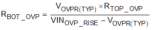
where
- VOVPR(TYP) = 1.15 V
- RTOP_OVP = 100 kΩ
- VINOVP_RISE = 5.4 V
In order to ensure the selected RBOT_OVP value is acceptable for both the minimum and maximum OVP rising threshold, use Equation 21. VINOVP_RISE(MIN) is selected as the highest possible value that VIN will reach during nominal operation. VINOVP_RISE(MAX) may be selected by the user as long as it is within the VIN of the Recommended Operating Conditions. These selections result in an allowable value of RBOT_OVP between 9.214 kΩ and 27.791 kΩ. The selected 27 kΩ-0.1% tolerance resistor satisfies these constraints, even when taking into account its tolerance.

where
- VOVPR(MAX) = 1.18 V
- RTOP_OVP = 100 kΩ
- Rtolerance = 0.01% = 0.001
- VINOVP_RISE(MAX) = 14 V
- VOVPR(MIN) = 1.11 V
- VINOVP_RISE(MIN) = VIN × (1 + tolerance) = 5.1 V
Since the OVP pin has hysteresis, the OVP falling threshold will be different than the rising threshold. Therefore, in order to ensure the selected RBOT_OVP value is acceptable for the OVP falling threshold, use Equation 22. VINOVP_FALL(MIN) and VINOVP_FALL(MAX) values may be selected using the same method as for VINOVP_RISE(MIN) and VINOVP_RISE(MAX). These selections results in an allowable RBOT_OVP value between of 9.128 kΩ and 27.154 kΩ. The selected 27 kΩ-0.1% tolerance resistor also satisfies these constraints, even when taking into account its tolerance.

where
- VOVPF(MAX) = 1.17 V
- RTOP_OVP = 100 kΩ
- Rtolerance = 0.001
- VINOVP_FALL(MAX) = 14 V
- VOVPF(MIN) = 1.09 V
- VINOVP_FALL(MIN) = VIN × (1 + tolerance) = 5.1 V
To summarize, using Equation 3 and Equation 4 with RTOP_OVP = 100 kΩ and RBOT_OVP = 27 kΩ, the eFuse will nominally go into overvoltage protection mode at 5.41 V and exit at 5.36 V. Taking into account the minimum and maximum OVP pin threshold and resistor tolerances, the switch will enter overvoltage protection mode between 5.21 V and 5.56 V and exit between 5.12 V and 5.51 V.