SLVSCJ8B November 2014 – January 2015
PRODUCTION DATA.
- 1 Features
- 2 Applications
- 3 Description
- 4 Typical Application Schematic
- 5 Revision History
- 6 Pin Configuration and Functions
- 7 Specifications
- 8 Detailed Description
- 9 Application and Implementation
- 10Power Supply Recommendations
- 11Layout
- 12Device and Documentation Support
- 13Mechanical, Packaging, and Orderable Information
封装选项
机械数据 (封装 | 引脚)
散热焊盘机械数据 (封装 | 引脚)
- DCY|4
订购信息
7 Specifications
7.1 Absolute Maximum Ratings
over operating free-air temperature range (unless otherwise noted)(1)| MIN | MAX | UNIT | ||
|---|---|---|---|---|
| Unregulated input voltage | IN(2)(3)(4) | –0.3 | 45 | V |
| Regulated output voltage | OUT(2)(3) | –0.3 | 7 | V |
| Operating junction temperature range, TJ | –40 | 150 | °C | |
| Storage temperature, Tstg | –65 | 150 | °C | |
(1) Stresses beyond those listed under Absolute Maximum Ratings may cause permanent damage to the device. These are stress ratings only, which do not imply functional operation of the device at these or any other conditions beyond those indicated under Recommended Operating Conditions. Exposure to absolute-maximum-rated conditions for extended periods may affect device reliability.
(2) All voltage values are with respect to the GND terminal.
(3) Absolute negative voltage on these pins must not to go below –0.3 V.
(4) Absolute maximum voltage, withstands 45 V for 200 ms.
7.2 ESD Ratings
| VALUE | UNIT | ||||
|---|---|---|---|---|---|
| V(ESD) | Electrostatic discharge | Human body model (HBM), per AEC Q100-002(1) | ±2000 | V | |
| Charged device model (CDM), per AEC Q100-011 | Other pins | ±500 | |||
| Corner pins (4 pin: 1, 3, and 4; 5 pin: 1, 3, 4, and 5) |
±750 | ||||
(1) AEC Q100-002 indicates HBM stressing is done in accordance with the ANSI/ESDA/JEDEC JS-001 specification.
7.3 Recommended Operating Conditions
over operating free-air temperature range (unless otherwise noted)| MIN | MAX | UNIT | ||
|---|---|---|---|---|
| VI | Unregulated input voltage | 4 | 40 | V |
| VO | Output voltage | 0 | 5.5 | V |
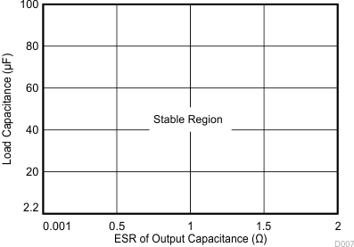
| CO | Output capacitor requirements(1) | 2.2 | 100 | µF |
| ESRCO | Output ESR requirements(2) | 0.001 | 2 | Ω |
| TJ | Operating junction temperature range | –40 | 150 | °C |
(1) The output capacitance range specified in this table is the effective value.
(2) Relevant ESR value at ƒ = 10 kHz.
7.4 Thermal Information
| THERMAL METRIC(1)(2) | DCY | DBV | UNIT | |
|---|---|---|---|---|
| 4 PINS | 5 PINS | |||
| RθJA | Junction-to-ambient thermal resistance | 64.2 | 210.4 | °C/W |
| RθJC(top) | Junction-to-case (top) thermal resistance | 46.8 | 126.1 | |
| RθJB | Junction-to-board thermal resistance | 13.3 | 38.4 | |
| ψJT | Junction-to-top characterization parameter | 6.3 | 16 | |
| ψJB | Junction-to-board characterization parameter | 13.2 | 37.5 | |
(1) The thermal data is based on the JEDEC standard high-K profile, JESD 51-7, 2s2p four layer board with 2-oz copper. The copper pad is soldered to the thermal land pattern. Also correct attachment procedure must be incorporated.
(2) For more information about traditional and new thermal metrics, see the IC Package Thermal Metrics application report, SPRA953.
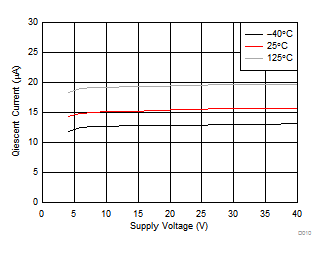
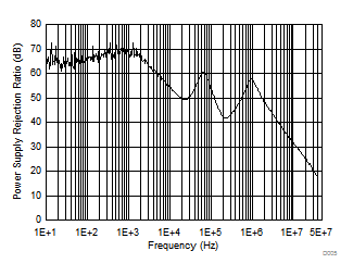
7.5 Electrical Characteristics
VIN = 14 V, 1 mΩ < ESR < 2 Ω, TJ = –40°C to 150 °C (unless otherwise noted)| PARAMETER | TEST CONDITIONS | MIN | TYP | MAX | UNIT | |
|---|---|---|---|---|---|---|
| SUPPLY VOLTAGE AND CURRENT (IN) | ||||||
| VI | Input voltage | Fixed 2.5-V output, IO = 1 mA | 4 | 40 | V | |
| Fixed 3.3-V output, IO = 1 mA | 4 | 40 | ||||
| Fixed 5-V output, IO = 1 mA | 5.5 | 40 | ||||
| IQ | Quiescent current | Fixed 2.5-V and 3.3-V version, VI = 4 to 40 V, Fixed 5-V version, VI = 5.5 to 40 V, IO = 0.2 mA |
15 | 25 | µA | |
| VIN(UVLO) | IN undervoltage detection | Ramp VI up until the output turns on | 3.65 | V | ||
| Ramp VI down until the output turns OFF | 3 | |||||
| REGULATED OUTPUT (OUT) | ||||||
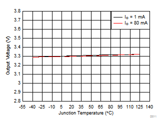
| VO | Regulated output | Fixed 2.5-V version, VI = 4 to 40 V, IO = 1 to 150 mA | –3% | 3% | ||
| Fixed 3.3-V version, VI = 5 to 40 V, IO = 1 to 150 mA | –3% | 3% | ||||
| Fixed 5-V version, VI = 6.5 to 40 V, IO = 1 to 150 mA | –3% | 3% | ||||
| ΔVO(ΔVI) | Line regulation | VI = 6 to 40 V, ∆VO, IO = 10 mA | 10 | mV | ||
| ΔVO(ΔIL) | Load regulation | IO = 1 to 150 mA, ∆VO | 20 | mV | ||
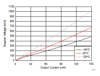
| VDROP | Dropout voltage | Fixed 2.5-V version, VI – VO, IO = 50 mA | 1.575 | V | ||
| Fixed 2.5-V version, VI – VO, IO = 100 mA | 1.575 | |||||
| Fixed 3.3-V version, VI – VO, IO = 50 mA | 799 | mV | ||||
| Fixed 3.3-V version, VI – VO, IO = 100 mA | 800 | |||||
| Fixed 5-V version, VI – VO, IO = 50 mA | 220 | 400 | ||||
| Fixed 5-V version, VI – VO, IO = 100 mA | 450 | 800 | ||||
| IO | Output current | VO in regulation | 0 | 150 | mA | |
| IOCL | Output current-limit | OUT short to ground | 150 | 500 | mA | |
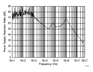
| PSRR | Power supply ripple rejection(1) | Vrip = 0.5 Vpp, Load = 10 mA, ƒ = 100 Hz, CO = 2.2 µF | 60 | dB | ||
| OPERATING TEMPERATURE RANGE | ||||||
| Tsd | Junction shutdown temperature | 175 | °C | |||
| Thys | Hysteresis of thermal shutdown | 25 | °C | |||
(1) Design Information—Not tested, ensured by characterization.
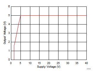
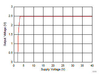
7.6 Typical Characteristics
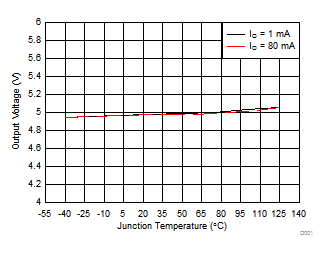
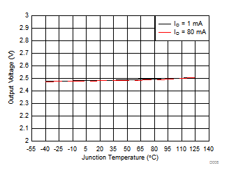
| VI = 14 V | ||
| IO = 0 mA | ||

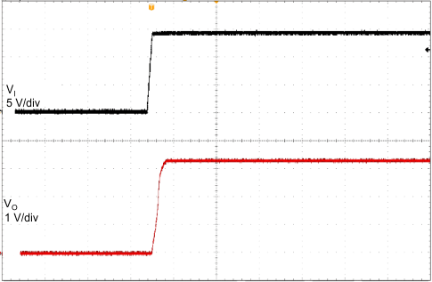
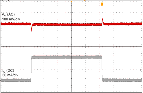
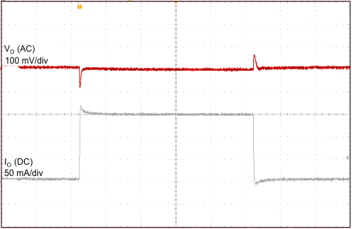
| IO = 10 mA | VI = 14 V | TA = 25°C |
| CO = 2.2 µF |
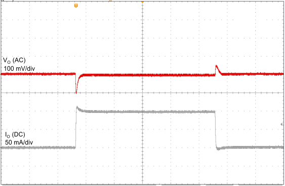
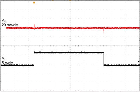
| VI = 14 V | CO = 2.2 µF | 1 ms/div |
| VO = 5 V | ||
| VI = 14 V | CO = 2.2 µF | 1 ms/div |
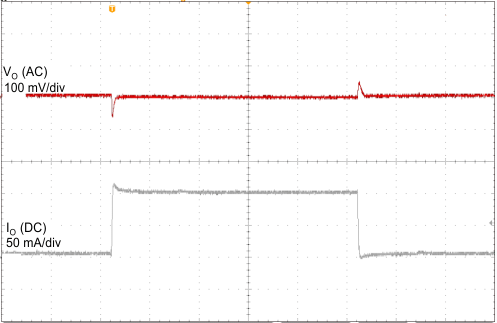
| VO = 2.5 V | ||
| VI = 14 V | CO = 2.2 µF | 1 ms/div |
| VO = 3.3 V | ||
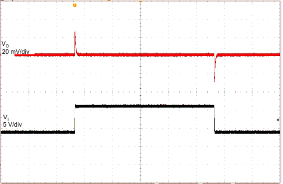
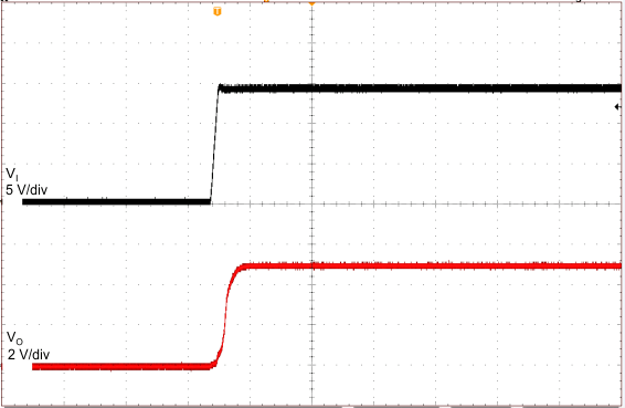
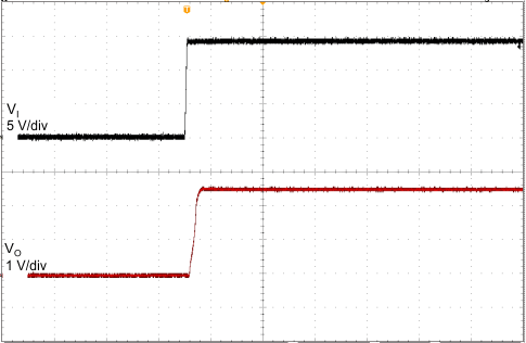
| VI = 9 to 16 V | CO = 2.2 µF | 1 ms/div |
| IO = 10 mA | ||
| VI = 9 to 16 V | CO = 2.2 µF | 1 ms/div |
| IO = 10 mA | ||
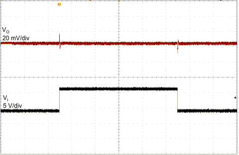
| CO = 2.2 µF, 400 µs/div | ||
| IO = 0 mA | ||
| IO = 0 mA | ||
| IO = 0.2 mA | ||
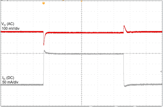
| IO = 100 mA | VI = 14 V | TA = 25°C |
| CO = 2.2 µF |
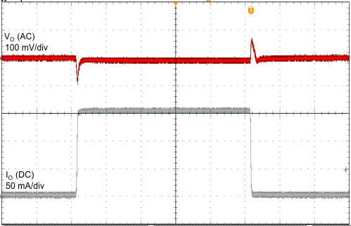
| VI = 14 V | CO = 2.2 µF | 1 ms/div |
| VO = 3.3 V | ||
| VI = 14 V | CO = 2.2 µF | 1 ms/div |
| VO = 5 V | ||
| VI = 14 V | CO = 2.2 µF | 1 ms/div |
| VO = 2.5 V |
| VI = 9 to 16 V | CO = 2.2 µF | 1 ms/div |
| IO = 10 mA | ||
| CO = 2.2 µF, 400 µs/div | ||
| CO = 2.2 µF, 400 µs/div | ||