SLVSCJ8B November 2014 – January 2015
PRODUCTION DATA.
- 1 Features
- 2 Applications
- 3 Description
- 4 Typical Application Schematic
- 5 Revision History
- 6 Pin Configuration and Functions
- 7 Specifications
- 8 Detailed Description
- 9 Application and Implementation
- 10Power Supply Recommendations
- 11Layout
- 12Device and Documentation Support
- 13Mechanical, Packaging, and Orderable Information
封装选项
机械数据 (封装 | 引脚)
散热焊盘机械数据 (封装 | 引脚)
- DCY|4
订购信息
8 Detailed Description
8.1 Overview
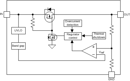
The TPS7B69xx-Q1 high-voltage linear regulator operates over a 4-V to 40-V input voltage range. The device has an output current capability of 150 mA and offers fixed output voltages of 2.5 V (TPS7B6925-Q1), 3.3 V (TPS7B6933-Q1) or 5 V (TPS7B6950-Q1). The device features a thermal shutdown and short-circuit protection to prevent damage during over-temperature and overcurrent conditions.
8.2 Functional Block Diagram
8.3 Feature Description
8.3.1 Input (IN)
The IN pin is a high-voltage-tolerant pin. A capacitor with a value higher than 0.1 µF is recommended to be connected close to this pin to better the transient performance.
8.3.2 Output (OUT)
The OUT pin is the regulated output based on the required voltage. The output has current limitation. During the initial power up, the regulator has a soft start incorporated to control the initial current through the pass element and the output capacitor.
In the event that the regulator drops out of regulation, the output tracks the input minus a drop based on the load current. When the input voltage drops below the UVLO threshold, the regulator shuts down until the input voltage recovers above the minimum startup level.
8.3.3 Output Capacitor Selection
For stable operation over the full temperature range and with load currents up to 150 mA, use a capacitor with an effective value between 2.2 µF and 100 µF and ESR smaller than 2 Ω. To better the load transient performance, an output capacitor, such as a ceramic capacitor with low ESR, is recommended.
8.3.4 Low-Voltage Tracking
At low input voltages, the regulator drops out of regulation and the output voltage tracks input minus a voltage based on the load current (IL) and switch resistor. This tracking allows for a smaller input capacitor and can possibly eliminate the need for a boost converter during cold-crank conditions.
8.3.5 Thermal Shutdown
The TPS7B69xx-Q1 family of devices incorporates a thermal-shutdown (TSD) circuit as a protection from overheating. For continuous normal operation, the junction temperature should not exceed the TSD trip point. If the junction temperature exceeds the TSD trip point, the output turns off. When the junction temperature falls below the TSD trip point minus the hysteresis of TSD, the output turns on again. This cycling limits the dissipation of the regulator, protecting it from damage as a result of overheating.
The purpose of the design of the internal protection circuitry of the TPS7B69xx-Q1 family of devices is for protection against overload conditions, not as a replacement for proper heat-sinking. Continuously running the TPS7B69xx-Q1 family of devices into thermal shutdown degrades device reliability.
8.4 Device Functional Modes
8.4.1 Operation With VI Less Than 4 V
The TPS7B69xx-Q1 family of devices operates with input voltages above 4 V. The maximum UVLO voltage is 3 V and the device operates at an input voltage above 4 V. The device can also operate at lower input voltages; no minimum UVLO voltage is specified. At input voltages below the actual UVLO, the device shuts down.
8.4.2 Operation With VI Greater Than 4 V
When VI is greater than 4 V, if the input voltage is higher than VO plus the dropout voltage, the output voltage is equal to the set value. Otherwise, the output voltage is equal to VI minus the dropout voltage.