SBVS313 June 2017 TPS7A85A
PRODUCTION DATA.
- 1 Features
- 2 Applications
- 3 Description
- 4 Revision History
- 5 Pin Configuration and Functions
- 6 Specifications
- 7 Detailed Description
-
8 Application and Implementation
- 8.1
Application Information
- 8.1.1
External Component Selection
- 8.1.1.1 Adjustable Operation
- 8.1.1.2 ANY-OUT Programmable Output Voltage
- 8.1.1.3 ANY-OUT Operation
- 8.1.1.4 Increasing ANY-OUT Resolution for LILO Conditions
- 8.1.1.5 Current Sharing
- 8.1.1.6 Recommended Capacitor Types
- 8.1.1.7 Input and Output Capacitor Requirements (CIN and COUT)
- 8.1.1.8 Feed-Forward Capacitor (CFF)
- 8.1.1.9 Noise-Reduction and Soft-Start Capacitor (CNR/SS)
- 8.1.2 Start-Up
- 8.1.3 AC and Transient Performance
- 8.1.4 DC Performance
- 8.1.5 Sequencing Requirements
- 8.1.6 Negatively Biased Output
- 8.1.7 Reverse Current
- 8.1.8 Power Dissipation (PD)
- 8.1.1
External Component Selection
- 8.2 Typical Applications
- 8.1
Application Information
- 9 Power-Supply Recommendations
- 10Layout
7 Detailed Description
7.1 Overview
The TPS7A85A is a high-current (4 A), low-noise (4.4 µVRMS), high accuracy (0.75%) low-dropout linear voltage regulator (LDO). These features make the device a robust solution to solve many challenging problems in generating a clean, accurate power supply.
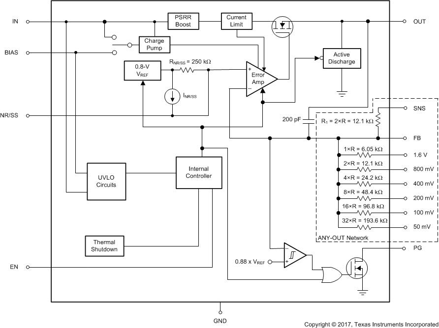
The TPS7A85A has several features that makes the device useful in a variety of applications. See Table 1 for a categorization of the functions shown in the Functional Block Diagram.
Table 1. Features
| VOLTAGE REGULATION | SYSTEM START-UP | INTERNAL PROTECTION |
|---|---|---|
| High accuracy | Programmable soft-start | Foldback current limit |
| Low-noise, high-PSRR output | No sequencing requirement between BIAS, IN and EN | Thermal shutdown |
| Fast transient response | Power-good output | |
| Start-up with negative bias on OUT |
Overall, these features make the TPS7A85A the component of choice due to its versatility and ability to generate a supply for most applications.
7.2 Functional Block Diagram

NOTE:
For the ANY-OUT network, the ratios between the values are highly accurate as a result of matching, but the actual resistance may vary significantly from the numbers listed.7.3 Feature Description
7.3.1 Voltage Regulation Features
7.3.1.1 DC Regulation
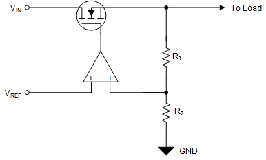
An LDO functions as a class-B amplifier in which the input signal is the internal reference voltage (VREF), as shown in Figure 46. VREF is designed to have a very low bandwidth at the input to the error amplifier through the use of a low-pass filter (VNR/SS).
As such, the reference can be considered as a pure dc input signal. The low output impedance of an LDO comes from the combination of the output capacitor and pass element. The pass element presents a high input impedance to the source voltage when operating as a current source. A positive LDO can only source current because of the class-B architecture.
This device achieves a maximum of 0.75% output voltage accuracy primarily because of the high-precision band-gap voltage (VBG) that creates VREF. The low dropout voltage (VDO) reduces the thermal power dissipation required by the device to regulate the output voltage at a given current level, which improves system efficiency. These features combine to make this device a good approximation of an ideal voltage source.

NOTE:
VOUT = VREF × (1 + R1 / R2).7.3.1.2 AC and Transient Response
The LDO responds quickly to a transient (large-signal response) on the input supply (line transient) or the output current (load transient) resulting from the LDO high-input impedance and low output-impedance across frequency. This same capability also means that the LDO has a high power-supply rejection ratio (PSRR) and, when coupled with a low internal noise-floor (Vn), the LDO approximates an ideal power supply in ac (small-signal) and large-signal conditions.
The choice of external component values optimizes the small- and large-signal response. The NR/SS capacitor (CNR/SS) and feed-forward capacitor (CFF) reduce the device noise floor and improve PSRR; see Optimizing Noise and PSRR for more information on optimizing the noise and PSRR performance.
7.3.2 System Start-Up Features
In many different applications, the power-supply output must turn on within a specific window of time to either ensure proper operation of the load or to minimize the loading on the input supply or other sequencing requirements. The LDO start-up is well-controlled and user-adjustable, solving the demanding requirements faced by many power-supply design engineers in a simple fashion.
7.3.2.1 Programmable Soft Start (NR/SS)
Soft start directly controls the output start-up time and indirectly controls the output current during start-up (inrush current).
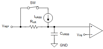
The external capacitor at the NR/SS pin (CNR/SS) sets the output start-up time by setting the rise time of the internal reference (VNR/SS), as shown in Figure 47.
 Figure 47. Simplified Soft-Start Circuit
7.3.2.2 Internal Sequencing
Controlling when a single power supply turns on can be difficult in a power distribution network (PDN) because of the high power levels inherent in a PDN, and the variations between all of the supplies. The LDO turnon and turnoff time is set by the enable circuit (EN) and undervoltage lockout circuits (UVLO1,2(IN) and UVLOBIAS), as shown in Figure 48 and Table 2.
 Figure 48. Simplified Turnon Control
Table 2. Internal Sequencing Functionality Table
| INPUT VOLTAGE | BIAS VOLTAGE | ENABLE STATUS | LDO STATUS | ACTIVE DISCHARGE | POWER GOOD |
|---|---|---|---|---|---|
| VIN ≥ VUVLO_1,2(IN) | VBIAS ≥ VUVLO(BIAS) | EN = 1 | On | Off | PG = 1 when VOUT ≥ VIT(PG) |
| EN = 0 | Off | On | PG = 0 | ||
| VBIAS < VUVLO(BIAS) + VHYS(BIAS) | EN = don't care | Off | On (1) | ||
| VIN < VUVLO_1,2(IN) – VHYS1,2(IN) | BIAS = don't care | Off | |||
| IN = don't care | VBIAS ≥ VUVLO(BIAS) | Off |
7.3.2.2.1 Enable (EN)
The enable signal (VEN) is an active-high digital control that enables the LDO when the enable voltage is past the rising threshold (VEN ≥ VIH(EN)) and disables the LDO when the enable voltage is below the falling threshold (VEN ≤ VIL(EN)). The exact enable threshold is between VIH(EN) and VIL(EN) because EN is a digital control. Connect EN to VIN if enable functionality is not desired.
7.3.2.2.2 Undervoltage Lockout (UVLO) Control
The UVLO circuits respond quickly to glitches on IN or BIAS and attempts to disable the output of the device if either of these rails collapse.
The local input capacitance prevents severe brownouts in most applications; see Undervoltage Lockout (UVLO) for more details.
7.3.2.2.3 Active Discharge
When EN or UVLO is low, the device connects a resistor of several hundred ohms from VOUT to GND, discharging the output capacitance.
Do not rely on the active discharge circuit for discharging large output capacitors when the input voltage drops below the targeted output voltage. Current flows from the output to the input (reverse current) when VOUT > VIN, which can cause damage to the device (when VOUT > VIN + 0.3 V); see Reverse Current for more details.
7.3.2.3 Power-Good Output (PG)
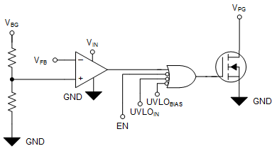
The PG signal provides an easy solution to meet demanding sequencing requirements because PG signals when the output nears its nominal value. PG can be used to signal other devices in a system when the output voltage is near, at, or above the set output voltage (VOUT(nom)). A simplified schematic is shown in Figure 49.
The PG signal is an open-drain digital output that requires a pullup resistor to a voltage source and is active high. The PG circuit sets the PG pin into a high-impedance state to indicate that the power is good.
Using a large feed-forward capacitor (CFF) delays the output voltage and, because the PG circuit monitors the FB pin, the PG signal can indicate a false positive. A simple solution to this scenario is to use an external voltage detector device, such as the TPS3890; see Feed-Forward Capacitor (CFF) for more information.
 Figure 49. Simplified PG Circuit
7.3.3 Internal Protection Features
In many applications, fault events can occur that damage devices in the system. Short circuits and excessive heat are the most common fault events for power supplies. The TPS7A85A implements circuitry to protect the device and the load during these events. Continuously operating in these fault conditions or above a junction temperature of 125°C is not recommended because the long-term reliability of the device is reduced.
7.3.3.1 Foldback Current Limit (ICL)
The internal current limit circuit protects the LDO against high load-current faults or shorting events. During a current-limit event, the LDO sources constant current. As a result, the output voltage falls with decreased load impedance. Thermal shutdown can activate during a current limit event because of the high power dissipation typically found in these conditions. To ensure proper operation of the current limit, minimize the inductances to the input and load. Continuous operation in current limit is not recommended.
7.3.3.2 Thermal Protection (Tsd)
The thermal shutdown circuit protects the LDO against excessive heat in the system, resulting from current limit or high ambient temperature.
The output of the LDO turns off when the LDO temperature (junction temperature, TJ) exceeds the rising thermal shutdown temperature. The output turns on again after TJ decreases below the falling thermal shutdown temperature.
A high power dissipation across the device, combined with a high ambient temperature (TA), can cause TJ to be greater than or equal to Tsd, which triggers the thermal shutdown and causing the output to fall to 0 V. The LDO can cycle on and off when thermal shutdown is reached under these conditions.
7.4 Device Functional Modes
Table 3 lists a comparison between the regulation and disabled operation.
Table 3. Device Functional Modes Comparison
| OPERATING MODE | PARAMETER | ||||
|---|---|---|---|---|---|
| VIN | VBIAS | EN | IOUT | TJ | |
| Regulation(1) | VIN > VOUT(nom) + VDO | VBIAS ≥ VUVLO(BIAS)(3) | VEN > VIH(EN) | IOUT < ICL | TJ ≤ TJ(maximum) |
| Disabled(2) | VIN < VUVLO_1,2(IN) | VBIAS < VUVLO(BIAS) | VEN < VIL(EN) | TJ > Tsd | |
| Current limit operation | IOUT ≥ ICL | ||||
7.4.1 Regulation
The device regulates the output to the nominal output voltage when all the conditions in Table 3 are met.
7.4.2 Disabled
When disabled, the pass device is turned off, the internal circuits are shut down, and the output voltage is actively discharged to ground by an internal resistor from the output to ground. See Active Discharge for additional information.