ZHCSBR4A April 2014 – June 2014 TPS7A8101-Q1
PRODUCTION DATA.
7 Specifications
7.1 Absolute Maximum Ratings
Over operating free-air temperature range (unless otherwise noted).(1)| MIN | MAX | UNIT | ||
|---|---|---|---|---|
| Voltage | IN | –0.3 | 7 | V |
| FB/SNS, NR | –0.3 | 3.6 | V | |
| EN | –0.3 | VI + 0.3(2) | V | |
| OUT | –0.3 | 7 | V | |
| Current | OUT | Internally Limited | A | |
| Operating junction temperature, TJ | –55 | 150 | °C | |
(1) Stresses beyond those listed under Absolute Maximum Ratings may cause permanent damage to the device. These are stress ratings only, and functional operation of the device at these or any other conditions beyond those indicated is not implied. Exposure to absolute-maximum-rated conditions for extended periods my affect device reliability.
(2) V(EN) absolute maximum rating is VI + 0.3 V or + 7 V, whichever is smaller.
7.2 Handling Ratings
| MIN | MAX | UNIT | ||||
|---|---|---|---|---|---|---|
| Tstg | Storage temperature range | –55 | 150 | °C | ||
| V(ESD) | Electrostatic discharge | Human body model (HBM), per AEC Q100-002, classification level H2(1) | –2 | 2 | kV | |
| Charged device model (CDM), per JEDEC specification JESD22-C101, classification level C4B | Corner pins (1, 4, 5, and 8) |
–750 | 750 | V | ||
| Other pins | –500 | 500 | ||||
(1) AEC Q100-002 indicates HBM stressing is done in accordance with the ANSI/ESDA/JEDEC JS-001 Specification.
7.3 Recommended Operating Conditions
Over operating free-air temperature range (unless otherwise noted)| MIN | MAX | UNIT | ||
|---|---|---|---|---|
| VI | Input voltage | 2.2 | 6.5 | V |
| IO | Output current | 0 | 1 | A |
| TA | Operating free air temperature | –40 | 125 | °C |
7.4 Thermal Information
| THERMAL METRIC(1) | DRB | UNIT | |
|---|---|---|---|
| (8 PINS) | |||
| RθJA | Junction-to-ambient thermal resistance | 45.7 | °C/W |
| RθJC(top) | Junction-to-case (top) thermal resistance | 53.1 | |
| RθJB | Junction-to-board thermal resistance | 21.2 | |
| ψJT | Junction-to-top characterization parameter | 0.9 | |
| ψJB | Junction-to-board characterization parameter | 21.4 | |
| RθJC(bot) | Junction-to-case (bottom) thermal resistance | 5.2 | |
(1) For more information about traditional and new thermal metrics, see the IC Package Thermal Metrics application report, SPRA953A.
7.5 Electrical Characteristics
Over the temperature range of –40°C ≤ TA, TJ ≤ 125°C, VI = VOnom + 0.5 V or 2.2 V (whichever is greater), IO = 1 mA, V(EN) = 2.2 V, C(OUT) = 4.7 μF, C(NR) = 0.01 μF, and C(BYPASS) = 0 μF, unless otherwise noted. The device is tested at VO = 0.8 V and VO = 6 V. Typical values are at TJ = 25°C.| PARAMETER | TEST CONDITIONS | MIN | TYP | MAX | UNIT | |||
|---|---|---|---|---|---|---|---|---|
| VI | Input voltage range(1) | 2.2 | 6.5 | V | ||||
| V(NR) | Internal reference | 0.79 | 0.8 | 0.81 | V | |||
| VO | Output voltage range | 0.8 | 6 | V | ||||
| Output accuracy(2) | VO + 0.5 V ≤ VI ≤ 6 V, VI ≥ 2.5 V, 100 mA ≤ IO ≤ 500 mA, 0°C ≤ TJ ≤ 85°C |
–2% | 2% | |||||
| VO + 0.5 V ≤ VI ≤ 6.5 V, VI ≥ 2.2 V, 100 mA ≤ IO ≤ 1 A |
–3% | ±0.3% | 3% | |||||
| ΔVO(ΔVI) | Line regulation | VOnom + 0.5 V ≤ VI ≤ 6.5 V, VI ≥ 2.2 V, IO = 100 mA |
150 | μV/V | ||||
| ΔVO(ΔIL) | Load regulation | 100 mA ≤ IO ≤ 1 A | 2 | μV/mA | ||||
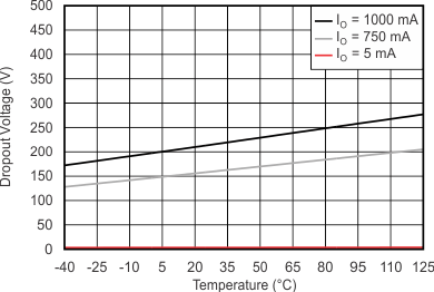
| VDO | Dropout voltage(3) | VO + 0.5 V ≤ VI ≤ 6.5 V, VI ≥ 2.2 V, IO = 500 mA, V(FB/SNS) = GND |
250 | mV | ||||
| VO + 0.5 V ≤ VI ≤ 6.5 V, VI ≥ 2.5 V, IO = 750 mA, V(FB/SNS) = GND |
350 | mV | ||||||
| VO + 0.5 V ≤ VI ≤ 6.5 V, VI ≥ 2.5 V, IO = 1 A, V(FB/SNS) = GND |
500 | mV | ||||||
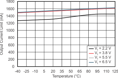
| IL | Output current-limit | VO = 0.85 × VOnom, VI ≥ 3.3 V | 1100 | 1400 | 2000 | mA | ||
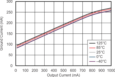
| I(GND) | Ground pin current | IO = 1 mA | 60 | 100 | μA | |||
| IO = 1 A | 350 | μA | ||||||
| IL(sd) | Shutdown current (I(GND)) | V(EN) ≤ 0.4 V, VI ≥ 2.2 V, RL = 1 kΩ, 0°C ≤ TJ ≤ 125°C |
0.2 | 2.5 | μA | |||
| I(FB/SNS) | Feedback pin current | VI = 6.5 V, V(FB/SNS) = 0.8 V | 0.02 | 1 | μA | |||
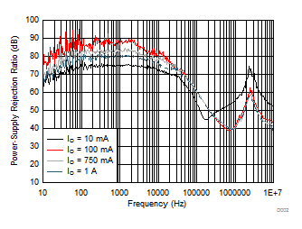
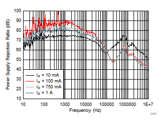
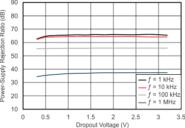
| PSRR | Power-supply rejection ratio | VI = 4.3 V, VO = 3.3 V, IO = 750 mA |
ƒ = 100 Hz | 80 | dB | |||
| ƒ = 1 kHz | 82 | dB | ||||||
| ƒ = 10 kHz | 78 | dB | ||||||
| ƒ = 100 kHz | 60 | dB | ||||||
| ƒ = 1 MHz | 54 | dB | ||||||
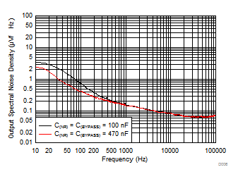
| Vn | Output noise voltage | BW = 100 Hz to 100 kHz, VI = 3.8 V, VO = 3.3 V, IO = 100 mA, C(NR) = C(BYPASS) = 470 nF |
23.5 | μVRMS | ||||
| V(EN)H | Enable high (enabled) | 2.2 V ≤ VI ≤ 3.6 V, RL = 1 kΩ | 1.2 | V | ||||
| 3.6 V < VI ≤ 6.5 V, RL = 1 kΩ | 1.35 | V | ||||||
| V(EN)L | Enable low (shutdown) | RL = 1 kΩ | 0 | 0.4 | V | |||
| I(EN) | Enable pin current, enabled | VI = V(EN) = 6.5 V | 0.02 | 1 | μA | |||
| tst | Startup time | VOnom = 3.3 V, VO = 0% to 90% VOnom, R1 = 3.3 kΩ, C(OUT) = 10 μF, C(NR) = 470 nF |
80 | ms | ||||
| UVLO | Undervoltage lockout | VI rising, RL = 1 kΩ | 1.86 | 2 | 2.1 | V | ||
| Hysteresis | VI falling, RL = 1 kΩ | 75 | mV | |||||
| Tsd | Thermal shutdown temperature | Shutdown, temperature increasing | 160 | °C | ||||
| Reset, temperature decreasing | 140 | °C | ||||||
(1) Minimum VI = VO + VDO or 2.2 V, whichever is greater.
(2) The TPS7A8101-Q1 does not include external resistor tolerances and it is not tested at this condition: VO = 0.8 V, 4.5 V ≤ VI ≤ 6.5 V, and 750 mA ≤ IO ≤ 1 A because the power dissipation is greater than the maximum rating of the package.
(3) VDO is not measured for fixed output voltage devices with VO < 1.7 V because minimum VI = 2.2 V.
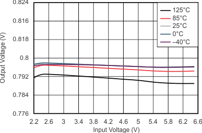
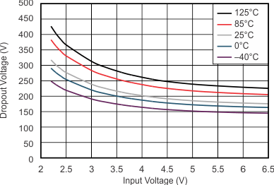
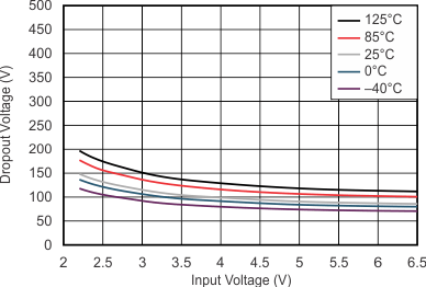
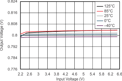
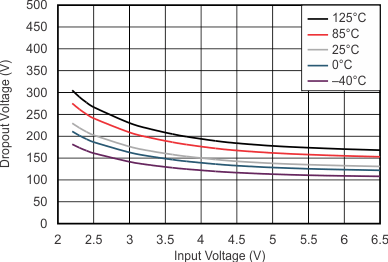
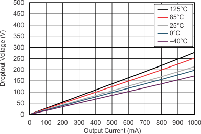
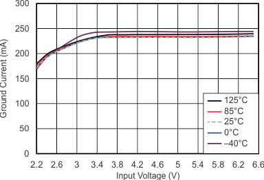
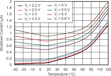
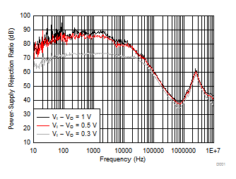
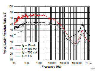
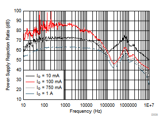
7.6 Typical Characteristics
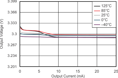
At VOnom = 3.3 V, VI = VOnom + 0.5 V or 2.2 V (whichever is greater), IO = 100 mA, V(EN) = VI, C(IN) = 1 μF, C(OUT) = 4.7 μF, and C(NR) = 0.01 μF; all temperature values refer to TJ, unless otherwise noted.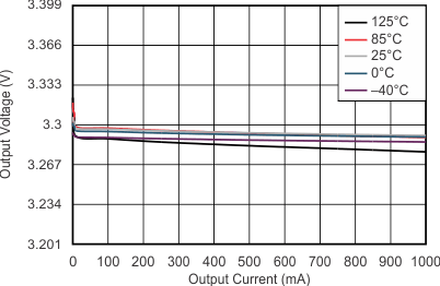
| NOTE: The Y-axis shows 1% VO per division | ||
| VO = 0.8 V | IO = 750 mA | |
| NOTE: The Y-axis shows 1% VO per division | ||
| IO = 1 A | ||
| IO = 500 mA | ||
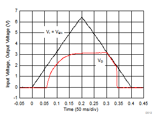
| VI = 3.6 V | ||
| VO = VI – 0.5 V |
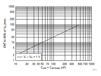
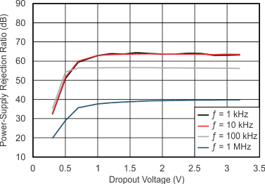
| VI – VO = 1 V | C(IN) = 0 F | C(OUT) = 10 µF |
| C(NR) = C(BYPASS) = 470 nF | ||
| VI – VO = 1 V | C(IN) = 0 F | C(OUT) = 10 µF |
| C(NR) = C(BYPASS) = 470 nF | ||
| IO = 100 mA | C(IN) = 0 F |
| VI – VO = 0.5 V | C(OUT) = 10 µF | C(IN) = 10 µF | |
| 24.09 µVRMS (C(NR) = C(BYPASS) = 100 nF) | |||
| 23.54 µVRMS (C(NR) = C(BYPASS) = 470 nF) | |||
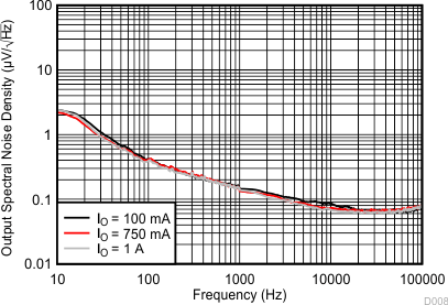
| 23.54 µVRMS (IO = 100 mA) | C(IN) = 10 µF | VI – VO = 0.5 V |
| 23.71 µVRMS (IO = 750 mA) | C(NR) = 470 nF | C(OUT) = 10 µF |
| 22.78 µVRMS (IO = 1 A) | C(BYPASS) = 470 nF | |
| Using the same value of C(NR) and C(BYPASS) in the X-Axis |
| IO = 100 mA → 1 A → 100 mA | ||
| RL = 33 Ω | C(NR) = 470 nF | C(BYPASS) = 470 nF | ||
| C(OUT) = 10 µF | C(IN) = 10 µF | |||
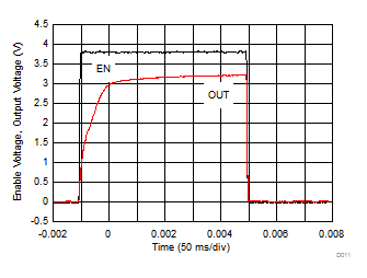
| (1) The internal reference requires approximately 80 ms of rampup time (see Startup) from the enable event; therefore, VO fully reaches the target output voltage of 3.3 V in 80 ms from startup. | ||||
| NOTE: The Y-axis shows 1% VO per division | ||
| VO = 0.8 V | IO = 5 mA | |
| NOTE: The Y-axis shows 1% VO per division | ||
| IO = 750 mA | ||
| VI = 3.6 V | ||
| VO = 0.8 V | IO = 750 mA | |
| V(EN) = 0.4 V | ||
| C(NR) = C(BYPASS) = 470 nF | C(OUT) = 10 µF | C(IN) = 0 F |
| VI – VO = 0.5 V | C(IN) = 0 F | C(OUT) = 10 µF |
| C(NR) = C(BYPASS) = 470 nF | ||
| VI – VO = 0.5 V | C(IN) = 0 F | C(OUT) = 10 µF |
| C(NR) = C(BYPASS) = 470 nF | ||
| IO = 750 mA | C(IN) = 0 F |
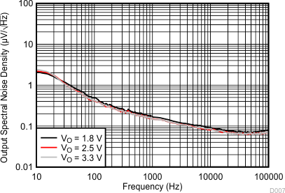
| 25.89 µVRMS (VO = 1.8 V) | C(IN) = 10 µF | VI – VO = 0.5 V |
| 23.54 µVRMS (VO = 2.5 V) | C(NR) = 470 nF | C(OUT) = 10 µF |
| 23.54 µVRMS (VO = 3.3 V) | C(BYPASS) = 470 nF | |
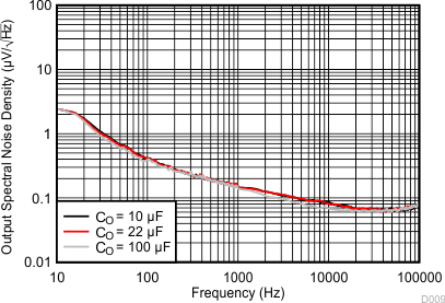
| 23.54 µVRMS (CO = 10 µF) | C(IN) = 10 µF | VI – VO = 0.5 V |
| 23.91 µVRMS (CO = 22 µF) | C(NR) = 470 nF | C(OUT) = 10 µF |
| 22.78 µVRMS (CO = 100 µF) | C(BYPASS) = 470 nF | |
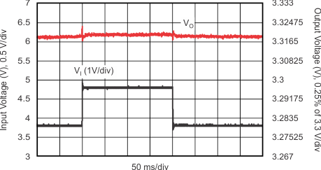
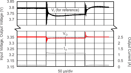
| VI = 3.8 V → 4.8 V → 3.8 V | ||
| IO = 500 mA | ||
| RL = 33 Ω | C(NR) = 470 nF | C(BYPASS) = 470 nF |
| C(OUT) = 10 µF | C(IN) = 10 µF |