ZHCSHB6A November   2019  – March 2020 TPS7A53

PRODUCTION DATA.  

  1. 特性
  2. 应用
  3. 说明
    1.     Device Images
      1.      为射频组件供电
      2.      为数字负载供电
  4. 修订历史记录
  5. Pin Configuration and Functions
    1.     Pin Functions
  6. Specifications
    1. 6.1 Absolute Maximum Ratings
    2. 6.2 ESD Ratings
    3. 6.3 Recommended Operating Conditions
    4. 6.4 Thermal Information
    5. 6.5 Electrical Characteristics
    6. 6.6 Typical Characteristics
  7. Detailed Description
    1. 7.1 Overview
    2. 7.2 Functional Block Diagram
    3. 7.3 Feature Description
      1. 7.3.1 Voltage Regulation Features
        1. 7.3.1.1 DC Regulation
        2. 7.3.1.2 AC and Transient Response
      2. 7.3.2 System Start-Up Features
        1. 7.3.2.1 Programmable Soft Start (NR/SS Pin)
        2. 7.3.2.2 Internal Sequencing
          1. 7.3.2.2.1 Enable (EN)
          2. 7.3.2.2.2 Undervoltage Lockout (UVLO) Control
          3. 7.3.2.2.3 Active Discharge
        3. 7.3.2.3 Power-Good Output (PG)
      3. 7.3.3 Internal Protection Features
        1. 7.3.3.1 Foldback Current Limit (ICL)
        2. 7.3.3.2 Thermal Protection (Tsd)
    4. 7.4 Device Functional Modes
      1. 7.4.1 Regulation
      2. 7.4.2 Disabled
      3. 7.4.3 Current Limit Operation
  8. Application and Implementation
    1. 8.1 Application Information
      1. 8.1.1  Recommended Capacitor Types
        1. 8.1.1.1 Input and Output Capacitor Requirements (CIN and COUT)
        2. 8.1.1.2 Noise-Reduction and Soft-Start Capacitor (CNR/SS)
        3. 8.1.1.3 Feed-Forward Capacitor (CFF)
      2. 8.1.2  Soft Start and Inrush Current
      3. 8.1.3  Optimizing Noise and PSRR
      4. 8.1.4  Charge Pump Noise
      5. 8.1.5  Current Sharing
      6. 8.1.6  Adjustable Operation
      7. 8.1.7  Power-Good Operation
      8. 8.1.8  Undervoltage Lockout (UVLO) Operation
      9. 8.1.9  Dropout Voltage (VDO)
      10. 8.1.10 Device Behavior During Transition From Dropout Into Regulation
      11. 8.1.11 Load Transient Response
      12. 8.1.12 Reverse Current Protection Considerations
      13. 8.1.13 Power Dissipation (PD)
      14. 8.1.14 Estimating Junction Temperature
      15. 8.1.15 TPS7A52EVM Thermal Analysis
    2. 8.2 Typical Application
      1. 8.2.1 Design Requirements
      2. 8.2.2 Detailed Design Procedure
      3. 8.2.3 Application Curves
  9. Power Supply Recommendations
  10. 10Layout
    1. 10.1 Layout Guidelines
      1. 10.1.1 Board Layout
    2. 10.2 Layout Example
  11. 11器件和文档支持
    1. 11.1 器件支持
      1. 11.1.1 开发支持
        1. 11.1.1.1 评估模块
        2. 11.1.1.2 Spice 模型
      2. 11.1.2 器件命名规则
    2. 11.2 文档支持
      1. 11.2.1 相关文档
    3. 11.3 接收文档更新通知
    4. 11.4 社区资源
    5. 11.5 商标
    6. 11.6 静电放电警告
    7. 11.7 Glossary
  12. 12机械、封装和可订购信息

封装选项

机械数据 (封装 | 引脚)
散热焊盘机械数据 (封装 | 引脚)
订购信息

Power-Good Output (PG)

The PG signal provides an easy solution to meet demanding sequencing requirements because PG signals when the output nears its nominal value. PG can be used to signal other devices in a system when the output voltage is near, at, or above the set output voltage (VOUT(nom)). Figure 43 shows a simplified schematic.

The PG signal is an open-drain digital output that requires a pullup resistor to a voltage source and is active high. The PG circuit sets the PG pin into a high-impedance state to indicate that the power is good.

Using a large feed-forward capacitor (CFF) delays the output voltage and, because the PG circuit monitors the FB pin, the PG signal can indicate a false positive.
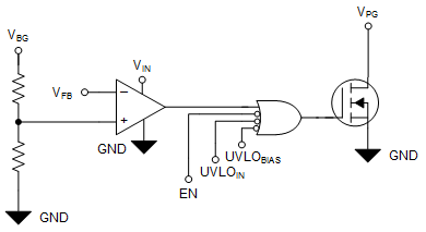
TPS7A53 ai_pg_circuit_sbvs291.gifFigure 43. Simplified PG Circuit