ZHCS516B December   2011  – November 2018 TPS7A4101

PRODUCTION DATA.  

  1. 特性
  2. 应用
  3. 说明
    1.     Device Images
      1.      典型应用图
  4. 修订历史记录
  5. Pin Configuration and Functions
    1.     Pin Functions
  6. Specifications
    1. 6.1 Absolute Maximum Ratings
    2. 6.2 ESD Ratings
    3. 6.3 Recommended Operating Conditions
    4. 6.4 Thermal Information
    5. 6.5 Electrical Characteristics
    6. 6.6 Typical Characteristics
  7. Detailed Description
    1. 7.1 Overview
    2. 7.2 Functional Block Diagram
    3. 7.3 Feature Description
      1. 7.3.1 Enable Pin Operation
      2. 7.3.2 Thermal Protection
    4. 7.4 Device Functional Modes
      1. 7.4.1 Normal Operation
      2. 7.4.2 Dropout Operation
      3. 7.4.3 Disabled
  8. Application and Implementation
    1. 8.1 Application Information
      1. 8.1.1 Adjustable Operation
      2. 8.1.2 Transient Voltage Protection
    2. 8.2 Typical Application
      1. 8.2.1 Design Requirements
      2. 8.2.2 Detailed Design Procedure
        1. 8.2.2.1 Capacitor Recommendations
        2. 8.2.2.2 Input and Output Capacitor Requirements
        3. 8.2.2.3 Bypass Capacitor Requirements
        4. 8.2.2.4 Maximum AC Performance
        5. 8.2.2.5 Transient Response
      3. 8.2.3 Application Curve
  9. Power Supply Recommendations
  10. 10Layout
    1. 10.1 Layout Guidelines
      1. 10.1.1 Thermal Considerations
      2. 10.1.2 Power Dissipation
      3. 10.1.3 Package Mounting
    2. 10.2 Layout Example
  11. 11器件和文档支持
    1. 11.1 接收文档更新通知
    2. 11.2 社区资源
    3. 11.3 商标
    4. 11.4 静电放电警告
    5. 11.5 术语表
  12. 12机械、封装和可订购信息

封装选项

机械数据 (封装 | 引脚)
散热焊盘机械数据 (封装 | 引脚)
订购信息

Typical Characteristics

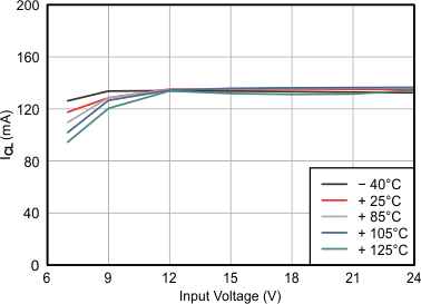
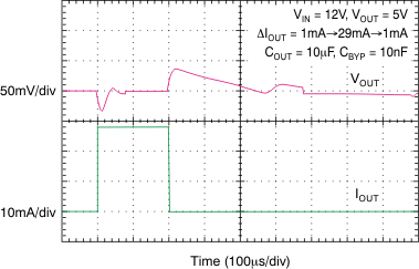
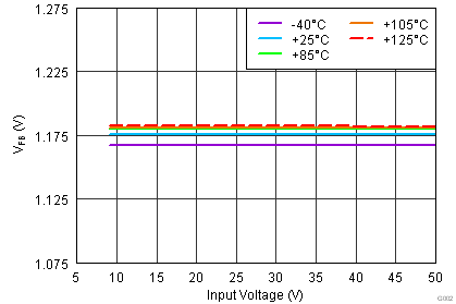
at TJ = –40°C to 125°C, VIN = VOUT(NOM) + 2 V or VIN = 9 V (whichever is greater), VEN = VIN, IOUT = 100 µA, CIN = 1 µF, COUT = 4.7 µF, and FB tied to OUT (unless otherwise noted)
TPS7A4101 tc_load_trans_bvs162.gif
Figure 1. Load Transient Response
TPS7A4101 G002_BVS183.png
Figure 3. Feedback Voltage
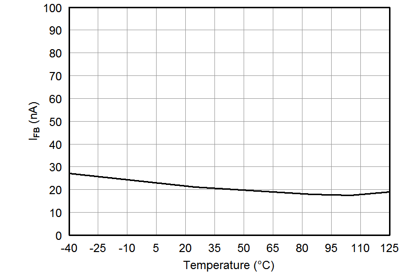
TPS7A4101 tc_ifb_bvs162.png
Figure 5. Feedback Current
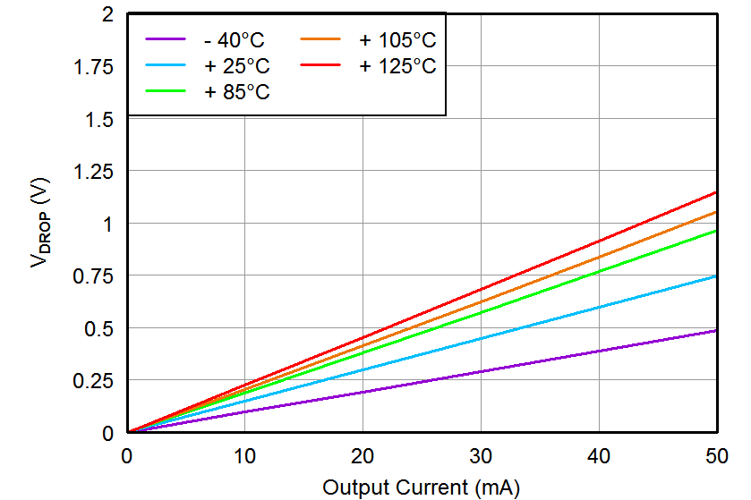
TPS7A4101 tc_vdo_bvs162.png
Figure 7. Dropout Voltage
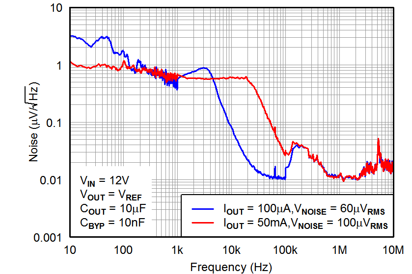
TPS7A4101 tc_noise_bvs162.png
Figure 9. Output Spectral Noise Density
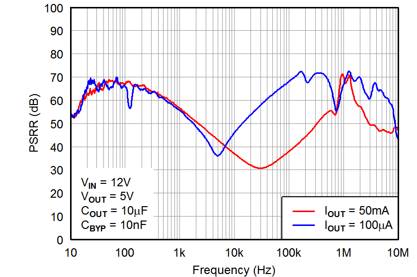
TPS7A4101 tc_psrr_bvs162.png
Figure 11. Power-Supply Rejection Ratio
TPS7A4101 G001_BVS183.png
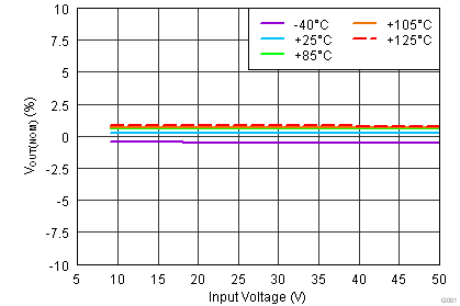
Figure 2. Line Regulation
TPS7A4101 G003_BVS183.png
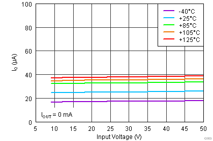
Figure 4. Quiescent Current vs Input Voltage
TPS7A4101 tc_ignd_bvs162.png
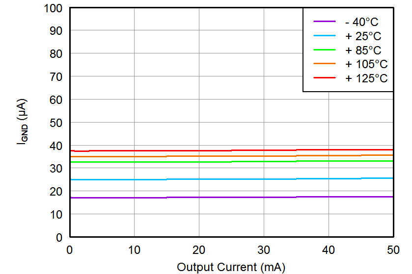
Figure 6. Ground Current
TPS7A4101 tc_ven_threshold_bvs162.gif
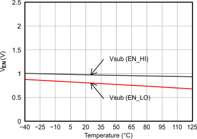
Figure 8. Enable Threshold Voltage
TPS7A4101 tc_ilim_bvs162.gif
Figure 10. Current Limit