ZHCSJ50C December   2018  – December 2022 TPS7A25

PRODUCTION DATA  

  1. 特性
  2. 应用
  3. 说明
  4. Revision History
  5. Pin Configuration and Functions
  6. Specifications
    1. 6.1 Absolute Maximum Ratings
    2. 6.2 ESD Ratings
    3. 6.3 Recommended Operating Conditions
    4. 6.4 Thermal Information
    5. 6.5 Electrical Characteristics
  7. Typical Characteristics
  8. Detailed Description
    1. 8.1 Overview
    2. 8.2 Functional Block Diagrams
    3. 8.3 Feature Description
      1. 8.3.1 Output Enable
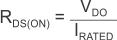
      2. 8.3.2 Dropout Voltage
      3. 8.3.3 Current Limit
      4. 8.3.4 Undervoltage Lockout (UVLO)
      5. 8.3.5 Thermal Shutdown
      6. 8.3.6 Power Good
      7. 8.3.7 Active Overshoot Pulldown Circuitry
    4. 8.4 Device Functional Modes
      1. 8.4.1 Device Functional Mode Comparison
      2. 8.4.2 Normal Operation
      3. 8.4.3 Dropout Operation
      4. 8.4.4 Disabled
        1.       Application and Implementation
          1. 9.1 Application Information
            1. 9.1.1 Adjustable Device Feedback Resistors
            2. 9.1.2 Recommended Capacitor Types
            3. 9.1.3 Input and Output Capacitor Requirements
            4. 9.1.4 Reverse Current
            5. 9.1.5 Feed-Forward Capacitor (CFF)
            6. 9.1.6 Power Dissipation (PD)
            7. 9.1.7 Estimating Junction Temperature
            8. 9.1.8 Special Consideration for Line Transients
          2. 9.2 Typical Application
            1. 9.2.1 Design Requirements
            2. 9.2.2 Detailed Design Procedure
              1. 9.2.2.1 Transient Response
              2. 9.2.2.2 Selecting Feedback Divider Resistors
              3. 9.2.2.3 Thermal Dissipation
            3. 9.2.3 Application Curve
          3. 9.3 Power Supply Recommendations
          4. 9.4 Layout
            1. 9.4.1 Layout Guidelines
            2. 9.4.2 Layout Examples
  9. Device and Documentation Support
    1. 9.1 Device Support
      1. 9.1.1 Device Nomenclature
    2. 9.2 Documentation Support
      1. 9.2.1 Related Documentation
    3. 9.3 接收文档更新通知
    4. 9.4 支持资源
    5. 9.5 Trademarks
    6. 9.6 Electrostatic Discharge Caution
    7. 9.7 术语表
  10. 10Mechanical, Packaging, and Orderable Information
    1. 10.1 Mechanical Data

封装选项

请参考 PDF 数据表获取器件具体的封装图。

机械数据 (封装 | 引脚)
  • DRV|6
散热焊盘机械数据 (封装 | 引脚)
订购信息

Dropout Voltage

Dropout voltage (VDO) is defined as the input voltage minus the output voltage (VIN – VOUT) at the rated output current (IRATED), where the pass transistor is fully on. IRATED is the maximum IOUT listed in the Recommended Operating Conditions table. The pass transistor is in the ohmic or triode region of operation, and acts as a switch. The dropout voltage indirectly specifies a minimum input voltage greater than the nominal programmed output voltage at which the output voltage is expected to stay in regulation. If the input voltage falls to less than the nominal output regulation, then the output voltage falls as well.

For a CMOS regulator, the dropout voltage is determined by the drain-source on-state resistance (RDS(ON)) of the pass transistor. Therefore, if the linear regulator operates at less than the rated current, the dropout voltage for that current scales accordingly. Use Equation 1 to calculate the RDS(ON) of the device.

Equation 1. GUID-7027C40F-0CB9-4692-A8D9-4F58620D7A08-low.gif