ZHCSHN3D February   2018  – August 2019 TPS7A05

PRODUCTION DATA.  

  1. 特性
  2. 应用
  3. 说明
    1.     Device Images
      1.      典型应用电路
      2.      接地电流与输出电流间的关系
  4. 修订历史记录
  5. Pin Configuration and Functions
    1.     Pin Functions
  6. Specifications
    1. 6.1 Absolute Maximum Ratings
    2. 6.2 ESD Ratings
    3. 6.3 Recommended Operating Conditions
    4. 6.4 Thermal Information
    5. 6.5 Electrical Characteristics
    6. 6.6 Switching Characteristics
    7. 6.7 Typical Characteristics
  7. Detailed Description
    1. 7.1 Overview
    2. 7.2 Functional Block Diagram
    3. 7.3 Feature Description
      1. 7.3.1 Excellent Transient Response
      2. 7.3.2 Active Discharge
      3. 7.3.3 Low IQ in Dropout
      4. 7.3.4 Undervoltage Lockout (UVLO)
      5. 7.3.5 Enable
      6. 7.3.6 Internal Foldback Current Limit
      7. 7.3.7 Thermal Shutdown
    4. 7.4 Device Functional Modes
      1. 7.4.1 Normal Mode
      2. 7.4.2 Dropout Mode
      3. 7.4.3 Disable Mode
  8. Application and Implementation
    1. 8.1 Application Information
      1. 8.1.1 Recommended Capacitor Types
      2. 8.1.2 Input and Output Capacitor Requirements
      3. 8.1.3 Special Considerations When Ramping Down VIN and Enable
      4. 8.1.4 Load Transient Response
      5. 8.1.5 Dropout Voltage
        1. 8.1.5.1 Behavior When Transitioning From Dropout Into Regulation
        2. 8.1.5.2 Behavior of Output Resulting From Line Transient When in Dropout
      6. 8.1.6 Undervoltage Lockout (UVLO) Operation
      7. 8.1.7 Power Dissipation (PD)
        1. 8.1.7.1 Estimating Junction Temperature
        2. 8.1.7.2 Recommended Area for Continuous Operation
    2. 8.2 Typical Application
      1. 8.2.1 Design Requirements
      2. 8.2.2 Design Considerations
      3. 8.2.3 Application Curve
  9. Power Supply Recommendations
  10. 10Layout
    1. 10.1 Layout Guidelines
    2. 10.2 Layout Example
  11. 11器件和文档支持
    1. 11.1 器件支持
      1. 11.1.1 Spice 模型
      2. 11.1.2 器件命名规则
    2. 11.2 文档支持
      1. 11.2.1 相关文档
    3. 11.3 接收文档更新通知
    4. 11.4 社区资源
    5. 11.5 商标
    6. 11.6 静电放电警告
    7. 11.7 Glossary
  12. 12机械、封装和可订购信息

封装选项

机械数据 (封装 | 引脚)
散热焊盘机械数据 (封装 | 引脚)
订购信息

Special Considerations When Ramping Down VIN and Enable

Care must be taken when ramping down voltage on the IN and EN pins to power-down the device when the operating free-air temperature is less than 15°C. The minimum ramp-down time for the IN pin is 10 ms. The minimum ramp-down time for the EN pin is 100 µs. Ramping at faster rates can cause the regulator to exhibit undesired startup behavior on the next power-on.

If VIN is ramped down faster than 10 ms, the next startup may exhibit a partial startup, shutoff, followed by a normal soft-start startup. Figure 48 shows this response.
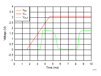
TPS7A05 D040_SBVS254.gifFigure 48. Partial Startup, Shutdown, Normal Startup With VEN = VIN

If the EN pin is ramped down faster than 100 µs, the next startup may exhibit a delay time of up to 130 ms before the output ramps up with a normal soft-start startup. Figure 49 shows this delay.
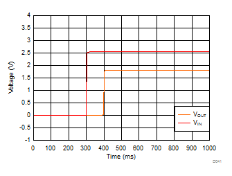
TPS7A05 D041_SBVS254.gifFigure 49. Long Delay to Startup With VEN = VIN

Fast ramp downs of VIN and the EN pin charge internal high-impedance nodes in the device, which take extended time to discharge below 15°C. To avoid these startup behaviors, follow the recommended minimum ramp down times for VIN and the EN pin.