SBVS115D August 2008 – January 2015 TPS782
PRODUCTION DATA.
- 1 Features
- 2 Applications
- 3 Description
- 4 Revision History
- 5 Pin Configuration and Functions
- 6 Specifications
- 7 Detailed Description
- 8 Application and Implementation
- 9 Power Supply Recommendations
- 10Layout
- 11Device and Documentation Support
- 12Mechanical, Packaging, and Orderable Information
封装选项
机械数据 (封装 | 引脚)
散热焊盘机械数据 (封装 | 引脚)
- DRV|6
订购信息
5 Pin Configuration and Functions
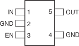
DRV PACKAGE
2-mm x 2-mm SON-6
(TOP VIEW)
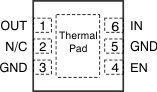
Pin Functions
| PIN | I/O | DESCRIPTION | ||
|---|---|---|---|---|
| NAME | DRV | DDC | ||
| OUT | 1 | 5 | O | Regulated output voltage pin. A small (1-μF) ceramic capacitor is needed from this pin to ground to assure stability. See the Input and Output Capacitor Requirements in the Application and Implementation section for more details. |
| NC | 2 | — | — | No internal connection. |
| EN | 4 | 3 | I | Enable pin. Drive this pin over 1.2 V to turn on the regulator. Drive this pin below 0.4 V to put the regulator into shutdown mode, reducing operating current to 18 nA typical. |
| GND | 3, 5 | 2, 4 | — | Ground pin. Tie all ground pins to ground for proper operation. |
| IN | 6 | 1 | I | Input pin. For stable operation, place a small, 0.1-µF capacitor from this pin to ground; typical input capacitor = 1.0 µF. Tie back both input and output capacitor grounds to the IC ground, with no significant impedance between them. |
| Thermal pad | Thermal pad | — | — | Connect the thermal pad to ground. |