ZHCSAL3R December   2005  – April 2017 TPS74401

PRODUCTION DATA.  

  1. 特性
  2. 应用
  3. 说明
  4. 修订历史记录
  5. Pin Configuration and Functions
  6. Specifications
    1. 6.1 Absolute Maximum Ratings
    2. 6.2 ESD Ratings
    3. 6.3 Recommended Operating Conditions
    4. 6.4 Thermal Information
    5. 6.5 Electrical Characteristics
    6. 6.6 Timing Requirements
    7. 6.7 Typical Characteristics
  7. Detailed Description
    1. 7.1 Overview
    2. 7.2 Functional Block Diagram
    3. 7.3 Feature Description
      1. 7.3.1 Enable, Shutdown
      2. 7.3.2 Power-Good (VQFN Package Only)
      3. 7.3.3 Internal Current Limit
      4. 7.3.4 Thermal Protection
    4. 7.4 Device Functional Modes
      1. 7.4.1 Normal Operation
      2. 7.4.2 Dropout Operation
      3. 7.4.3 Disabled
    5. 7.5 Programming
      1. 7.5.1 Programmable Soft-Start
      2. 7.5.2 Sequencing Requirements
  8. Application and Implementation
    1. 8.1 Application Information
      1. 8.1.1 Input, Output, and Bias Capacitor Requirements
      2. 8.1.2 Transient Response
      3. 8.1.3 Dropout Voltage
      4. 8.1.4 Output Noise
    2. 8.2 Typical Applications
      1. 8.2.1 Setting the TPS74401
        1. 8.2.1.1 Design Requirements
        2. 8.2.1.2 Detailed Design Procedure
        3. 8.2.1.3 Application Curves
      2. 8.2.2 Using an Auxiliary Bias Rail
      3. 8.2.3 Without an Auxiliary Bias
  9. Power Supply Recommendations
  10. 10Layout
    1. 10.1 Layout Guidelines
    2. 10.2 Layout Example
    3. 10.3 Power Dissipation
    4. 10.4 Thermal Considerations
  11. 11器件和文档支持
    1. 11.1 器件支持
      1. 11.1.1 开发支持
        1. 11.1.1.1 评估模块
        2. 11.1.1.2 Spice 模型
    2. 11.2 文档支持
      1. 11.2.1 相关文档 
    3. 11.3 接收文档更新通知
    4. 11.4 社区资源
    5. 11.5 商标
    6. 11.6 静电放电警告
    7. 11.7 Glossary
  12. 12机械、封装和可订购信息

封装选项

机械数据 (封装 | 引脚)
散热焊盘机械数据 (封装 | 引脚)
订购信息

Pin Configuration and Functions

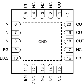
RGW, RGR Package
5-mm × 5-mm and 3.5-mm × 3.5-mm, 20-Pin VQFN
Top View
TPS74401 po_rgw_bvs066.gif
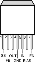
KTW Package
7-Pin DDPAK
Top View
TPS74401 po_ktw_bvs066.gif

Pin Functions

PIN I/O DESCRIPTION
NAME KTW RGW, RGR
BIAS 6 10 I Bias input voltage for error amplifier, reference, and internal control circuits.
A 1-µF or larger bias capacitor is recommended for optimal performance.
If IN is connected to BIAS, use a 4.7 µF or larger capacitor.
EN 7 11 I Enable pin. Driving this pin high enables the regulator. Driving this pin low puts the regulator into shutdown mode. This pin must not be left floating.
FB 2 16 I This pin is the feedback connection to the center tap of an external resistor divider network that sets the output voltage. This pin must not be left floating.
GND 4 12 Ground
IN 5 5–8 I Unregulated input to the device.
An input capacitor of 1 µF or greater is recommended for optimal performance.
NC N/A 2–4, 13, 14, 17 No connection. This pin can be left floating or connected to GND to allow better thermal contact to the top-side plane.
OUT 3 1, 18–20 O Regulated output voltage. No capacitor is required on this pin for stability, but is recommended for optimal performance.
PAD/TAB Must be soldered to the ground plane for increased thermal performance.
Internally connected to ground.
PG N/A 9 O Power-good (PG) is an open-drain, active-high output that indicates the status of VOUT. When VOUT exceeds the PG trip threshold, the PG pin goes into a high-impedance state. When VOUT is below this threshold, the pin is driven to a low-impedance state. Connect a pullup resistor from 10 kΩ to 1 MΩ from this pin to a supply up to 5.5 V. The supply can be higher than the input voltage.
Alternatively, the PG pin can be left floating if output monitoring is not necessary.
SS 1 15 Soft-start pin. A capacitor connected on this pin to ground sets the start-up time.
If this pin is left floating, the regulator output soft-start ramp time is typically 100 µs.