ZHCSD88B October   2014  – February 2019 TPS735-Q1

PRODUCTION DATA.  

  1. 特性
  2. 应用
  3. 说明
    1.     Device Images
      1.      典型应用
  4. 修订历史记录
  5. Pin Configuration and Functions
    1.     Pin Functions
  6. Specifications
    1. 6.1 Absolute Maximum Ratings
    2. 6.2 ESD Ratings
    3. 6.3 Recommended Operating Conditions
    4. 6.4 Thermal Information
    5. 6.5 Electrical Characteristics
    6. 6.6 Typical Characteristics
  7. Detailed Description
    1. 7.1 Overview
    2. 7.2 Functional Block Diagram
    3. 7.3 Feature Description
      1. 7.3.1 Internal Current-Limit
      2. 7.3.2 Shutdown
      3. 7.3.3 Dropout Voltage
      4. 7.3.4 Startup and Noise Reduction Capacitor
      5. 7.3.5 Transient Response
      6. 7.3.6 Undervoltage Lockout (UVLO)
      7. 7.3.7 Minimum Load
    4. 7.4 Device Functional Modes
      1. 7.4.1 Normal Operation
      2. 7.4.2 Dropout Operation
      3. 7.4.3 Disabled
  8. Application and Implementation
    1. 8.1 Application Information
    2. 8.2 Typical Application
      1. 8.2.1 Design Requirements
        1. 8.2.1.1 Input and Output Capacitor Requirements
        2. 8.2.1.2 Feedback Capacitor Requirements (TPS73501-Q1 only)
      2. 8.2.2 Detailed Design Procedure
        1. 8.2.2.1 Output Noise
      3. 8.2.3 Application Curves
  9. Power Supply Recommendations
  10. 10Layout
    1. 10.1 Layout Guidelines
      1. 10.1.1 Board Layout Recommendations to Improve PSRR and Noise Performance
      2. 10.1.2 Thermal Protection
      3. 10.1.3 Package Mounting
      4. 10.1.4 Power Dissipation
      5. 10.1.5 Estimating Junction Temperature
    2. 10.2 Layout Example
  11. 11器件和文档支持
    1. 11.1 器件支持
      1. 11.1.1 器件命名规则
    2. 11.2 文档支持
      1. 11.2.1 相关文档
    3. 11.3 接收文档更新通知
    4. 11.4 社区资源
    5. 11.5 商标
    6. 11.6 静电放电警告
    7. 11.7 术语表
  12. 12机械、封装和可订购信息

封装选项

请参考 PDF 数据表获取器件具体的封装图。

机械数据 (封装 | 引脚)
  • DRB|8
散热焊盘机械数据 (封装 | 引脚)
订购信息

Typical Application

Figure 15 shows the basic circuit connections for fixed-voltage models. Figure 16 gives the connections for the adjustable output version (TPS73501-Q1). Use the equation in Figure 16 to calculate the value of R1 and R2 for any output voltage.
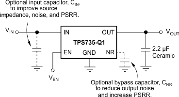
TPS735-Q1 ta_cir_fix_sbvs252.gifFigure 15. Typical Application Circuit for Fixed Voltage Versions
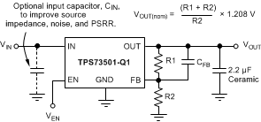
TPS735-Q1 ta_cir_adj_sbvs252.gifFigure 16. Typical Application Circuit for Adjustable Voltage Versions