SBVS340 June 2017 TPS715A-NM
PRODUCTION DATA.
- 1 Features
- 2 Applications
- 3 Description
- 4 Pin Configuration and Functions
- 5 Specifications
- 6 Detailed Description
- 7 Application and Implementation
- 8 Power Supply Recommendations
- 9 Layout
- 10Device and Documentation Support
- 11Mechanical, Packaging, and Orderable Information
9 Layout
9.1 Layout Guidelines
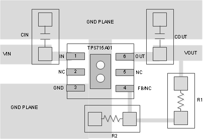
For best overall performance, place all circuit components on the same side of the printed-circuit-board and as near as practical to the respective LDO pin connections. Place ground return connections for the input and output capacitors as close to the GND pin as possible, using wide, component-side, copper planes. TI strongly discourages using vias and long traces to create LDO circuit connections to the input capacitor, output capacitor, or the resistor divider because doing so negatively affects system performance. This grounding and layout scheme minimizes inductive parasitics, and thereby reduces load-current transients, minimizes noise, and increases circuit stability. A ground reference plane is recommended to be embedded either in the PCB itself or located on the bottom side of the PCB opposite the components. This reference plane assures accuracy of the output voltage and shields the LDO from noise.
9.2 Layout Example
 Figure 21. Example Layout for the TPS715A01DRV
9.3 Power Dissipation
To ensure reliable operation, worst-case junction temperature must not exceed 125°C. This restriction limits the power dissipation the regulator can handle in any given application. To ensure the junction temperature is within acceptable limits, calculate the maximum allowable dissipation, PD(max), and the actual dissipation, PD, which must be less than or equal to PD(max).
The maximum-power-dissipation limit is determined using Equation 4.

where
- TJmax is the maximum allowable junction temperature
- RθJA is the thermal resistance junction-to-ambient for the package (see the Thermal Information table)
- TA is the ambient temperature
The regulator power dissipation is calculated using Equation 5.

For a higher power package version of the TPS715A-NM, see the TPS715A-NM.