ZHCSPJ3T May   2001  – December 2022 TPS715

PRODUCTION DATA  

  1. 特性
  2. 应用
  3. 说明
  4. Revision History
  5. Pin Configuration and Functions
  6. Specifications
    1. 6.1 Absolute Maximum Ratings
    2. 6.2 ESD Ratings
    3. 6.3 Recommended Operating Conditions
    4.     Thermal Information
    5. 6.4 Electrical Characteristics
    6. 6.5 Typical Characteristics
  7. Detailed Description
    1. 7.1 Overview
    2. 7.2 Functional Block Diagrams
    3. 7.3 Feature Description
      1. 7.3.1 Wide Supply Range
      2. 7.3.2 Low Quiescent Current
      3. 7.3.3 Dropout Voltage (VDO)
      4. 7.3.4 Current Limit
    4. 7.4 Device Functional Modes
      1. 7.4.1 Normal Operation
      2. 7.4.2 Dropout Operation
  8. Application and Implementation
    1. 8.1 Application Information
    2. 8.2 Typical Application
      1. 8.2.1 Detailed Design Procedure
        1. 8.2.1.1 Setting VOUT for the TPS71501 Adjustable LDO
        2. 8.2.1.2 External Capacitor Requirements
        3. 8.2.1.3 Input and Output Capacitor Requirements
        4. 8.2.1.4 Reverse Current
        5. 8.2.1.5 Feed-Forward Capacitor (CFF)
        6. 8.2.1.6 Power Dissipation (PD)
        7. 8.2.1.7 Estimating Junction Temperature
      2. 8.2.2 Application Curves
    3. 8.3 Best Design Practices
    4. 8.4 Power Supply Recommendations
    5. 8.5 Layout
      1. 8.5.1 Layout Guidelines
        1. 8.5.1.1 Power Dissipation
      2. 8.5.2 Layout Example
  9. Device and Documentation Support
    1. 9.1 Device Support
      1. 9.1.1 Development Support
        1. 9.1.1.1 Evaluation Module
        2. 9.1.1.2 Spice Models
      2. 9.1.2 Device Nomenclature
    2. 9.2 Documentation Support
      1. 9.2.1 Related Documentation
    3. 9.3 接收文档更新通知
    4. 9.4 支持资源
    5. 9.5 Trademarks
    6. 9.6 Electrostatic Discharge Caution
    7. 9.7 术语表
  10. 10Mechanical, Packaging, and Orderable Information

封装选项

机械数据 (封装 | 引脚)
散热焊盘机械数据 (封装 | 引脚)
订购信息

Power Dissipation

To ensure reliable operation, worst-case junction temperature must not exceed 125°C. This restriction limits the power dissipation the regulator can handle in any given application. To ensure the junction temperature is within acceptable limits, calculate the maximum allowable dissipation, PD(max), and the actual dissipation, PD, which must be less than or equal to PD(max).

The maximum-power-dissipation limit is determined using Equation 11:
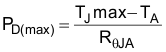
Equation 11. GUID-A7414963-F2CD-473F-B2E4-8FEC9707EB0A-low.gif

where

  • TJmax is the maximum allowable junction temperature
  • RθJA is the thermal resistance junction-to-ambient for the package (see the Section 6.4 table)
  • TA is the ambient temperature

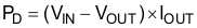
The regulator dissipation is calculated using Equation 12:

Equation 12. GUID-A0C34900-FD2A-4CE5-BEE1-161D53E261A7-low.gif

For a higher power package version of the TPS715, see the TPS715A.