ZHCSFC6 September 2015 TPS65233-1
PRODUCTION DATA.
- 1 特性
- 2 应用
- 3 说明
- 4 修订历史记录
- 5 Pin Configuration and Functions
- 6 Specifications
- 7 Detailed Description
- 8 Application and Implementation
- 9 Power Supply Recommendations
- 10Layout
- 11器件和文档支持
- 12机械、封装和可订购信息
6 Specifications
6.1 Absolute Maximum Ratings
over operating free-air temperature range, all voltages are with respect to GND (unless otherwise noted)(1)| MIN | MAX | UNIT | ||
|---|---|---|---|---|
| Voltage | VIN, LX, BOOST, VLNB | –1 | 30 | V |
| VCP | BOOST + 7 | |||
| LX | –1 | 30 | ||
| VCC, EN, FAULT, SCL, SDA, VCTRL, ISEL, EXTM | –0.3 | 7 | ||
| TCAP | –0.3 | 3.6 | ||
| PGND, AGND | –0.3 | 0.3 | ||
| Operating junction temperature, TJ | –40 | 125 | °C | |
| Storage temperature, Tstg | –55 | 150 | °C | |
(1) Stresses beyond those listed under Absolute Maximum Ratings may cause permanent damage to the device. These are stress ratings only, which do not imply functional operation of the device at these or any other conditions beyond those indicated under Recommended Operating Conditions. Exposure to absolute-maximum-rated conditions for extended periods may affect device reliability.
6.2 ESD Ratings
| VALUE | UNIT | |||
|---|---|---|---|---|
| V(ESD) | Electrostatic discharge | Human body model (HBM), per ANSI/ESDA/JEDEC JS-001, other pins(1) | 2000 | V |
| Human body model (HBM), per ANSI/ESDA/JEDEC JS-001, pin 13 (VLNB)(1) | 6000 | |||
| Charged device model (CDM), per JEDEC specification JESD22-C101, all pins(2) | 500 | |||
(1) JEDEC document JEP155 states that 500-V HBM allows safe manufacturing with a standard ESD control process.
(2) JEDEC document JEP157 states that 250-V CDM allows safe manufacturing with a standard ESD control process.
6.3 Recommended Operating Conditions
over operating free-air temperature range (unless otherwise noted)| MIN | NOM | MAX | UNIT | ||
|---|---|---|---|---|---|
| VIN | Input operating voltage | 4.5 | 20 | V | |
| TA | Junction temperature | –40 | 85 | °C | |
6.4 Thermal Information
| THERMAL METRIC(1) | TPS65233-1 | UNIT | |
|---|---|---|---|
| RTE (WQFN) | |||
| 16 PINS | |||
| RθJA | Junction-to-ambient thermal resistance | 43.4 | °C/W |
| RθJC(top) | Junction-to-case (top) thermal resistance | 45.6 | °C/W |
| RθJB | Junction-to-board thermal resistance | 15 | °C/W |
| ψJT | Junction-to-top characterization parameter | 0.6 | °C/W |
| ψJB | Junction-to-board characterization parameter | 15 | °C/W |
| RθJC(bot) | Junction-to-case (bottom) thermal resistance | 3.3 | °C/W |
(1) For more information about traditional and new thermal metrics, see the Semiconductor and IC Package Thermal Metrics application report, SPRA953.
6.5 Electrical Characteristics
TJ = –40°C to 125°C, VIN = 12 V, fSW = 1 MHz (unless otherwise noted)| PARAMETER | TEST CONDITIONS | MIN | TYP | MAX | UNIT | |
|---|---|---|---|---|---|---|
| INPUT SUPPLY | ||||||
| VIN | Input voltage range | VIN | 4.5 | 12 | 20 | V |
| IDDSDN | Shutdown supply current | EN = 0 | 160 | µA | ||
| IDDQ | LDO input quiescent current | EN = 1, IOUT = 0 A, VBOOST = 14 V, ILNB = 0 mA | 10.5 | mA | ||
| UVLO | VIN under voltage lockout | Rising VIN | 4.05 | 4.25 | 4.45 | V |
| Falling VIN | 3.6 | 3.8 | 4.1 | |||
| Hysteresis | 450 | mV | ||||
| OUTPUT VOLTAGE | ||||||
| VOUT | Regulated output voltage (non-I2C mode) | VCTRL = 1, SCL = 0, IOUT = 500 mA |
18 | V | ||
| VCTRL = 1, SCL = 1, IOUT = 500 mA |
18.2 | 18.6 | 19 | |||
| VCTRL = 0, SCL = 0, IOUT = 500 mA |
13 | |||||
| VCTRL = 0, SCL = 1, IOUT = 500 mA |
13.1 | 13.4 | 13.7 | |||
| VLINEREG | Line regulation-DC | VIN = 7.5 V to 16 V, IOUT = 500 mA |
0.2 | %/V | ||
| VLOADREG | Load regulation-DC | IOUT = (10-90%) × IOUTMAX | 0.7 | %/A | ||
| IOCP | Output short circuit current limit | RSEL = 200 kΩ, TJ = 25°C | 580 | 650 | 720 | mA |
| Tr, Tf | 13-V/18-V transition rising/falling time | CTCAP = 5.6 nF | 0.33 | ms | ||
| fSW | Boost switching frequency | 1040 | kHz | |||
| Ilimitsw | Switching current limit | VIN = 12 V, VOUT = 18.6 V | 3.2 | A | ||
| Rdson_LS | On resistance of low side FET on CH | VIN = 12 V | 120 | mΩ | ||
| Vdrop | Linear regulator voltage drop-out | IOUT = 500 mA | 0.8 | V | ||
| Irev | Reverse bias current | EN = 1, VLNB = 21 V | 50 | mA | ||
| Irev_dis | Disabled reverse bias current | EN = 0, VLNB = 21 V | 3 | mA | ||
| LOGIC SIGNALS | ||||||
| VEN | Enable threshold level | 1.15 | V | |||
| VENH | Enable threshold level hysteresis | 80 | mV | |||
| VLOGICh, VLOGICl | VCTRL, EXTM Logic threshold level | High level input voltage | 2 | V | ||
| Low level input voltage | 0.8 | |||||
| VOL FAULT | FAULT output low voltage | FAULT open drain, IOL= 1 mA | 0.4 | V | ||
| fI2C | Maximum I2C clock frequency | 400 | kHz | |||
| TONE | ||||||
| ftone | Tone frequency | 20 | 22 | 24 | kHz | |
| Atone | Tone amplitude | IOUT = 0 mA to 500 mA, COUT = 100 nF |
550 | 680 | 750 | mV |
| Dtone | Tone duty cycle | 45% | 50% | 55% | ||
| PROTECTION | ||||||
| TON | Over current protection on time | 4 | ms | |||
| TOFF | Over current protection off time | 128 | ms | |||
| THERMAL SHUTDOWN | ||||||
| TTRIP | Thermal shut down trip point | Rising temperature | 160 | °C | ||
| THYST | Thermal shut down hysteresis | 20 | °C | |||
| I2C READ BACK FAULT STATUS | ||||||
| VPGOOD | PGOOD trip levels | Feedback voltage low side rising | 95.3% | |||
| Feedback voltage low side falling | 94.7% | |||||
| Feedback voltage high side rising | 105.3% | |||||
| Feedback voltage high side falling | 104.7% | |||||
| Twarn | Temperature warning threshold | 125 | °C | |||
| I2C INTERFACE | ||||||
| VIH | SDA,SCL input high voltage | 2 | V | |||
| VIL | SDA,SCL input low voltage | 0.8 | V | |||
| II | Input current | SDA, SCL, VI = 0.4 V to 4.5 V | –10 | 10 | µA | |
| VOL | SDA output low voltage | SDA open drain, IOL = 2 mA | 0.4 | V | ||
| f(SCL) | Maximum SCL clock frequency | 400 | kHz | |||
| CB | Capacitance of one bus line (SCL and SDA) | 400 | pF | |||
6.6 I2C Interface Timing Requirements
| MIN | MAX | UNIT | |||
|---|---|---|---|---|---|
| tBUF | Bus free time between a STOP and START condition | 1.3 | µs | ||
| tHD, STA | Hold time (Repeated) START condition | 0.6 | µs | ||
| tSU, STO | Setup time for STOP condition | 0.6 | µs | ||
| tLOW | LOW period of the SCL clock | 1.3 | µs | ||
| tHIGH | HIGH period of the SCL clock | 0.6 | µs | ||
| tSU, STA | Setup time for a repeated START condition | 0.6 | µs | ||
| tSU, DAT | Data setup time | 0.1 | µs | ||
| tHD, DAT | Data hold time | 0 | 0.9 | µs | |
| tRCL | Rise time of SCL signal | 20 + 0.1CB | 300 | ns | |
| tRCL1 | Rise time of SCL signal after a repeated START condition and after an acknowledge BIT | 20 + 0.1CB | 300 | ns | |
| tf | Fall time of SCL signal | 20 + 0.1CB | 300 | ns | |
| tr | Rise time of SDA signal | 20 + 0.1CB | 300 | ns | |
| tFDA | Fall time of SDA signal | 20 + 0.1CB | 300 | ns | |
6.7 Switching Characteristics
over operating free-air temperature range (unless otherwise noted)| PARAMETER | TEST CONDITIONS | MIN | TYP | MAX | UNIT | |
|---|---|---|---|---|---|---|
| OUTPUT VOLTAGE | ||||||
| Tr, Tf | 13-V/18-V Transition rising falling time | Ccap = 5.6 nF | 0.33 | ms | ||
| TONE | ||||||
| Trtone | Tone rise time | IOUT = 0 to 500 mA, COUT = 100 nF | 10 | µs | ||
| Tftone | Tone fall time | IOUT = 0 to 500 mA, COUT = 100 nF | 10 | µs | ||
 Figure 1. I2C Interface Timing Diagram
6.8 Typical Characteristics
TA = 25°C, VIN = 12 V, fSW = 1 MHz, L = 4.7 µH, CBoost = 2 × 22 µF/35 V (unless otherwise noted)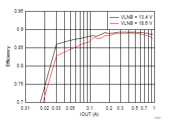
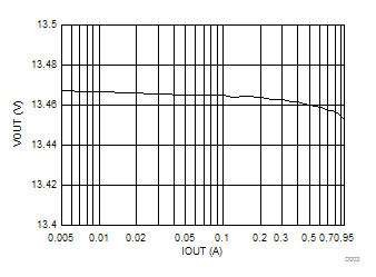
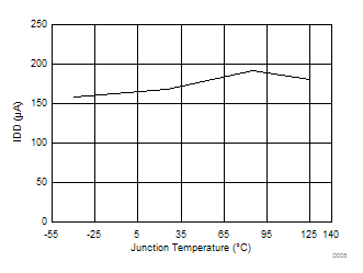
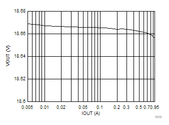
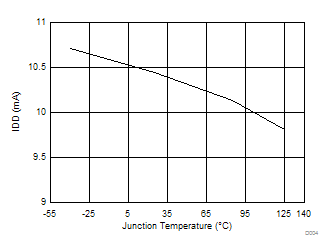
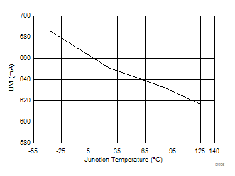
(ILIM = 650 mA)