ZHCSFC6 September   2015 TPS65233-1

PRODUCTION DATA.  

  1. 特性
  2. 应用
  3. 说明
  4. 修订历史记录
  5. Pin Configuration and Functions
  6. Specifications
    1. 6.1 Absolute Maximum Ratings
    2. 6.2 ESD Ratings
    3. 6.3 Recommended Operating Conditions
    4. 6.4 Thermal Information
    5. 6.5 Electrical Characteristics
    6. 6.6 I2C Interface Timing Requirements
    7. 6.7 Switching Characteristics
    8. 6.8 Typical Characteristics
  7. Detailed Description
    1. 7.1 Overview
    2. 7.2 Functional Block Diagram
    3. 7.3 Feature Description
      1. 7.3.1 Boost Converter
      2. 7.3.2 Linear Regulator and Current Limit
      3. 7.3.3 Charge Pump
      4. 7.3.4 Slew Rate Control
      5. 7.3.5 Short Circuit Protection, Hiccup, and Overtemperature Protection
    4. 7.4 Device Functional Modes
      1. 7.4.1 Tone Generation
      2. 7.4.2 Serial Interface
    5. 7.5 Programming
      1. 7.5.1 I2C Update Sequence
    6. 7.6 Register Map
      1. 7.6.1 Control Register 1 - Address: 0x00H
      2. 7.6.2 Control Register 2 - Address: 0x01H
      3. 7.6.3 Status Register 1 - Address: 0x02H
  8. Application and Implementation
    1. 8.1 Application Information
    2. 8.2 Typical Application
      1. 8.2.1 Detailed Design Procedure
        1. 8.2.1.1 Capacitor Selection
      2. 8.2.2 Application Curves
  9. Power Supply Recommendations
  10. 10Layout
    1. 10.1 Layout Guidelines
    2. 10.2 Layout Example
  11. 11器件和文档支持
    1. 11.1 社区资源
    2. 11.2 商标
    3. 11.3 静电放电警告
    4. 11.4 术语表
  12. 12机械、封装和可订购信息

封装选项

机械数据 (封装 | 引脚)
散热焊盘机械数据 (封装 | 引脚)
订购信息

10 Layout

10.1 Layout Guidelines

The TPS65233-1 is designed to layout in a 2-layer PCB. Figure 32 shows the recommended layout practice. It is critical to make sure the GND of the input capacitor, output capacitor, and boost converter are connected at one point on the same layer as shown below. PGND and AGND are in different regions and are connected to the thermal pad. Other components are connected to AGND.

10.2 Layout Example
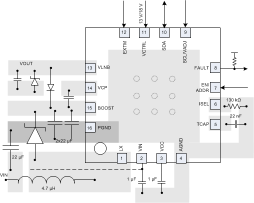
TPS65233-1 layout_SLVSD66.gif Figure 32. 2-Layer PCB Layout