ZHCSNM6A May 2021 – August 2021 TPS6521855
PRODUCTION DATA
- 1 特性
- 2 应用
- 3 说明
- 4 Revision History
- 5 Pin Configuration and Functions
- 6 Specifications
-
7 Detailed Description
- 7.1 Overview
- 7.2 Functional Block Diagram
- 7.3
Feature Description
- 7.3.1
Wake-Up and Power-Up and Power-Down Sequencing
- 7.3.1.1 Power-Up Sequencing
- 7.3.1.2 Power-Down Sequencing
- 7.3.1.3 Strobe 1 and Strobe 2
- 7.3.1.4 Supply Voltage Supervisor and Power-Good (PGOOD)
- 7.3.1.5 Internal LDO (INT_LDO)
- 7.3.1.6 Current Limited Load Switches
- 7.3.1.7 LDO1
- 7.3.1.8 UVLO
- 7.3.1.9 Power-Fail Comparator
- 7.3.1.10 DCDC3 and DCDC4 Power-Up Default Selection
- 7.3.1.11 I/O Configuration
- 7.3.1.12 Push Button Input (PB)
- 7.3.1.13 AC_DET Input (AC_DET)
- 7.3.1.14 Interrupt Pin (INT)
- 7.3.1.15 I2C Bus Operation
- 7.3.1
Wake-Up and Power-Up and Power-Down Sequencing
- 7.4 Device Functional Modes
- 7.5 Register Maps
- 8 Application and Implementation
- 9 Power Supply Recommendations
- 10Layout
- 11Device and Documentation Support
- 12Mechanical, Packaging, and Orderable Information
12.1.2 Tape and Reel Information
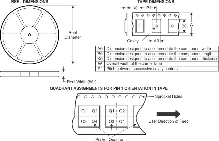
| Device | Package Type | Package Drawing | Pins | SPQ | Reel Diameter (mm) | Reel Width W1 (mm) | A0 (mm) | B0 (mm) | K0 (mm) | P1 (mm) | W (mm) | Pin1 Quadrant |
|---|---|---|---|---|---|---|---|---|---|---|---|---|
| TPS65218D0RSLR | VQFN | RSL | 48 | 2500 | 330.0 | 16.4 | 6.3 | 6.3 | 1.1 | 12.0 | 16.0 | Q2 |
| TPS65218D0PHP | HTQFP | PHP | 48 | 250 | 180.0 | 16.4 | 6.3 | 6.3 | 1.1 | 12.0 | 16.0 | Q2 |
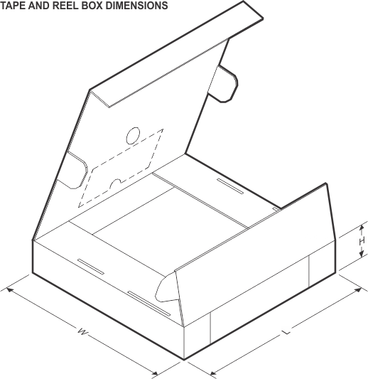
| Device | Package Type | Package Drawing | Pins | SPQ | Length (mm) | Width (mm) | Height (mm) |
|---|---|---|---|---|---|---|---|
| TPS65218D0RSLR | VQFN | RSL | 48 | 2500 | 367.0 | 367.0 | 38.0 |
| TPS65218D0PHP | HTQFP | PHP | 48 | 250 | 210.0 | 185.0 | 35.0 |