ZHCSQG4E March 2004 – April 2022 TPS65130 , TPS65131
PRODUCTION DATA
- 1 特性
- 2 应用
- 3 说明
- 4 Revision History
- 5 Pin Configuration and Functions
- 6 Specifications
- 7 Detailed Description
-
8 Applications and Implementation
- 8.1 Application Information
- 8.2
Typical Application
- 8.2.1 Design Requirements
- 8.2.2 Detailed Design Procedure
- 8.2.3 Analog Supply Filter
- 8.2.4 Application Curves
- 9 Layout
- 10Device and Documentation Support
- 11Mechanical, Packaging, and Orderable Information
封装选项
请参考 PDF 数据表获取器件具体的封装图。
机械数据 (封装 | 引脚)
- RGE|24
散热焊盘机械数据 (封装 | 引脚)
- RGE|24
订购信息
9.3 Thermal Considerations
Implementation of integrated circuits in low-profile and fine-pitch surface-mount packages typically requires special attention to power dissipation. Many system-dependent issues, such as thermal coupling, airflow, added heatsinks and convection surfaces, and the presence of heat-generating components affect the power-dissipation limits of a given component.
These three basic approaches enhance thermal performance:
- Improving the power dissipation capability of the PCB design.
- Improving the thermal coupling of the component to the PCB.
- Introducing airflow to the system.
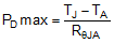
The recommended device junction temperature range, TJ, is –40°C to 125°C. The thermal resistance of the 24-pin QFN, 4–mm × 4–mm package (RGE) is RθJA = 34.1°C/W. The recommended operating ambient temperature range for the device is TA = –40°C to 85°C. Use Equation 13 to calculate the maximum power dissipation, PDmax, as a function of TA. In this equation, use TJ = 125°C to operate the device within the recommended temperature range, use TJ = TTS to determine the absolute maximum threshold when the device might go into thermal shutdown. If the maximum ambient temperature of the application is lower, more heat dissipation is possible.