ZHCSFB9B June 2016 – March 2019 TPS63070
PRODUCTION DATA.
- 1 特性
- 2 应用
- 3 说明
- 4 修订历史记录
- 5 Device Comparison Table
- 6 Pin Configuration and Functions
- 7 Specifications
- 8 Detailed Description
- 9 Application and Implementation
- 10Power Supply Recommendations
- 11Layout
- 12器件和文档支持
- 13机械、封装和可订购信息
8.4.1 Control Loop Description
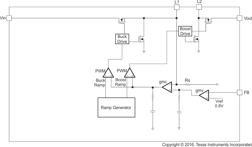
The controller circuit of the device is based on an average current mode topology. The average inductor current is regulated by a fast current regulator loop which is controlled by a voltage control loop.
The non inverting input of the transconductance amplifier gmv can be assumed to be constant. The output of gmv defines the average inductor current. The inductor current is reconstructed by measuring the current through the high side buck MOSFET. This current corresponds exactly to the inductor current in boost mode. In buck mode, the current is measured during the on-time of the same MOSFET. During the off-time, the current is reconstructed internally starting from the peak value reached at the end of the on-time cycle. The average current is then compared to the desired value and the difference, or current error, is amplified and compared to the sawtooth ramp of either the Buck or the Boost. Depending on which of the two ramps is crossed by the signal, either the Buck MOSFETs or the Boost MOSFETs are activated. When the input voltage is close to the output voltage, one buck cycle is followed by a boost cycle. In this condition, not more than three cycle in a row of the same mode are allowed. This control method in the buck-boost region ensures a robust control and the highest efficiency.
For an input voltage above 9 V, and Vout below 2.2 V, the switching frequency is reduced by a factor of 2 to keep the minimum on-time at a reasonable value. For short circuit protection, at an output voltage below 1.2V, the low side input FET and the high side output FET are not actively switched but their back-gate diode used for conduction.
TPS6307x also contains a negative current limit. This allows the inductor current to reverse and flow from the output to the input. This is required for forced PWM operation at low output current but also for applications that require a fairly high current from the output to the input like TEC (thermo electric cooling) applications where the TEC cell is placed between input and output of the converter,
 Figure 7. Average Current Mode Control