ZHCSBD3D July 2013 – August 2019 TPS63050 , TPS63051
PRODUCTION DATA.
- 1 特性
- 2 应用
- 3 说明
- 4 修订历史记录
- 5 Device Comparison Table
- 6 Pin Configuration and Functions
- 7 Specifications
- 8 Detailed Description
- 9 Application and Implementation
- 10Power Supply Recommendations
- 11Layout
- 12器件和文档支持
- 13机械、封装和可订购信息
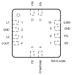
6 Pin Configuration and Functions
YFF Package
12-Pin DSBGA
Top View
Pin Functions
| PIN | I/O | DESCRIPTION | ||
|---|---|---|---|---|
| NAME | WCSP | HotRod | ||
| EN | A3 | 11 | I | Enable input. (1 enabled, 0 disabled). It must not be left floating |
| FB | D2 | 5 | I | Voltage feedback of adjustable versions, must be connected to VOUT on fixed output voltage versions1 |
| GND | B1 | 2,9 | Ground for Power stage and Control stage | |
| ILIM0 | B2 | 10 | I | Programmable inrush current limit input works together with lLIM1. See table on page 1.
It must not be left floating |
| ILIM1 | B3 | See (1) | I | Programmable inrush current limit input works together with lLIM0.
See 效率与输出电流间的关系 on page 1. Do not leave floating |
| L1 | A1 | 1 | Connection for Inductor | |
| L2 | C1 | 3 | Connection for Inductor | |
| PFM/PWM | C2 | 6 | I | 0 for PFM mode 1 for forced PWM mode. It must not be left floating |
| PG | C3 | 8 | O | Power good open drain output |
| SS | D3 | 7 | I | Adjustable Soft-Start. If left floating default soft-start time is set |
| VIN | A2 | 12 | I | Supply voltage for power stage and control stage |
| VOUT | D1 | 4 | O | Buck-boost converter output |
(1) Only available with DSBGA package, for VQFN package ILIM1 is internally connected to voltage level > VIH
