ZHCSLS6B August 2020 – June 2022 TPS628510 , TPS628511 , TPS628512 , TPS628513
PRODUCTION DATA
- 1 特性
- 2 应用
- 3 说明
- 4 Revision History
- 5 Device Comparison Table
- 6 Pin Configuration and Functions
- 7 Specifications
- 8 Parameter Measurement Information
-
9 Detailed Description
- 9.1 Overview
- 9.2 Functional Block Diagram
- 9.3 Feature Description
- 9.4
Device Functional Modes
- 9.4.1 Pulse Width Modulation (PWM) Operation
- 9.4.2 Power Save Mode Operation (PWM/PFM)
- 9.4.3 100% Duty-Cycle Operation
- 9.4.4 Current Limit and Short Circuit Protection
- 9.4.5 Foldback Current Limit and Short Circuit Protection
- 9.4.6 Output Discharge
- 9.4.7 Soft Start / Tracking (SS/TR)
- 9.4.8 Input Overvoltage Protection
- 10Application and Implementation
- 11Power Supply Recommendations
- 12Layout
- 13Device and Documentation Support
- 14Mechanical, Packaging, and Orderable Information
6 Pin Configuration and Functions
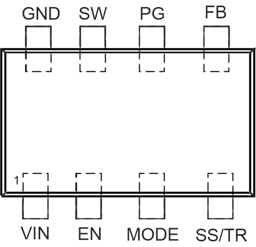
 Figure 6-1 8-Pin SOT583 DRL Package (Top
View)
Figure 6-1 8-Pin SOT583 DRL Package (Top
View)Table 6-1 Pin Functions
| PIN | I/O | DESCRIPTION | |
|---|---|---|---|
| NAME | NO. | ||
| EN | 2 | I | This is the enable pin of the device. Connect to logic low to disable the device. Pull high to enable the device. Do not leave this pin unconnected. |
| FB | 5 | I | Voltage feedback input. Connect the resistive output voltage divider to this pin. |
| GND | 8 | Ground pin | |
| MODE/SYNC | 3 | I | The device runs in PFM/PWM mode when this pin is pulled low. When the pin is pulled high, the device runs in forced PWM mode. Do not leave this pin unconnected. The mode pin can also be used to synchronize the device to an external frequency. See Section 7.5 for the detailed specification for the digital signal applied to this pin for external synchronization. |
| PG | 6 | O | Open-drain power-good output |
| SS/TR | 4 | I | Soft-Start / Tracking pin. An external capacitor connected from this pin to GND defines the rise time for the internal reference voltage. The pin can also be used as an input for tracking and sequencing - see Section 10.3.1 in this data sheet. |
| SW | 7 | This is the switch pin of the converter and is connected to the internal power MOSFETs. | |
| VIN | 1 | Power supply input. Make sure the input capacitor is connected as close as possible between the VIN pin and GND. | |