SLVSB63A December 2011 – March 2016 TPS62231-Q1 , TPS622314-Q1
PRODUCTION DATA.
- 1 Features
- 2 Applications
- 3 Description
- 4 Revision History
- 5 pPin Configuration and Functions
- 6 Specifications
- 7 Detailed Description
- 8 Application and Implementation
- 9 Power Supply Recommendations
- 10Layout
- 11Device and Documentation Support
- 12Mechanical, Packaging, and Orderable Information
10 Layout
10.1 Layout Guidelines
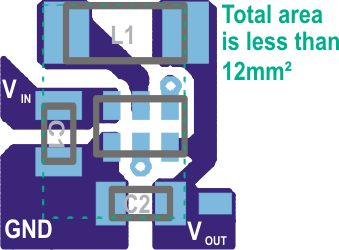
As for all switching power supplies, the layout is an important step in the design. Proper function of the device demands careful attention to PCB layout. Use care when designing the board layout to get the specified performance. If the layout is not done carefully, the regulator could show poor line regulation, load regulation, stability issues, and EMI problems. Providing a low-inductance, low-impedance ground path is critical. Therefore, use wide and short traces for the main current paths. Place the input capacitor as close as possible to the IC pins as well as the inductor and output capacitor.
Use a common power GND node and a different node for the Signal GND to minimize the effects of ground noise. Keep the common path to the GND PIN, which returns the small signal components and the high current of the output capacitors as short as possible to avoid ground noise. Connect the FB line to the output capacitor and route the line away from noisy components and traces (for example, SW line).
10.2 Layout Example
 Figure 25. Recommended PCB Layout for TPS6223x-Q1