SLVS941G April 2009 – August 2016 TPS62230
PRODUCTION DATA.
- 1 Features
- 2 Applications
- 3 Description
- 4 Revision History
- 5 Device Comparison Table
- 6 Pin Configuration and Functions
- 7 Specifications
- 8 Detailed Description
-
9 Application and Implementation
- 9.1 Application Information
- 9.2
Typical Application
- 9.2.1 Design Requirements
- 9.2.2 Detailed Design Procedure
- 9.2.3
Application Curves
- 9.2.3.1 VOUT = 1.1 V - TPS622311
- 9.2.3.2 VOUT = 1.2 V - TPS62232/TPS62235
- 9.2.3.3 VOUT = 1.8 V - TPS62231
- 9.2.3.4 VOUT = 1.85 V - TPS62236
- 9.2.3.5 VOUT = 2.5 V - TPS62230
- 9.2.3.6 VOUT = 3.0 V - TPS62233
- 9.2.3.7 Start-Up
- 9.2.3.8 PFM / PWM Operation
- 9.2.3.9 Peak-to-Peak Output Ripple Voltage
- 9.2.3.10 Power-Supply Rejection
- 9.2.3.11 Spurious Output Noise
- 9.2.3.12 Line Transient Response
- 9.2.3.13 Mode Transition
- 9.2.3.14 AC-Load Regulation
- 9.2.3.15 Load Transient Response
- 9.3 System Examples
- 10Power Supply Recommendations
- 11Layout
- 12Device and Documentation Support
- 13Mechanical, Packaging, and Orderable Information
7 Specifications
7.1 Absolute Maximum Ratings
over operating free-air temperature range (unless otherwise noted)(1)| MIN | MAX | UNIT | |||
|---|---|---|---|---|---|
| VIN | Voltage at VIN and SW pin(2) | –0.3 | 7 | V | |
| Voltage at EN, MODE pin(2) | –0.3 | VIN +0.3, ≤7 | V | ||
| Voltage at FB pin(2) | –0.3 | 3.6 | V | ||
| Peak output current | Internally limited | A | |||
| Power dissipation | Internally limited | ||||
| TJ | Operating junction Temperature Range | –40 | 150 | °C | |
| Tstg | Storage Temperature Range | –65 | 150 | °C | |
(1) Stresses beyond those listed under Absolute Maximum Ratings may cause permanent damage to the device. These are stress ratings only and functional operation of the device at these or any other conditions beyond those indicated under Recommended Operating Conditions is not implied. Exposure to absolute–maximum–rated conditions for extended periods may affect device reliability.
(2) All voltage values are with respect to network ground terminal.
7.2 ESD Ratings
| VALUE | UNIT | ||||
|---|---|---|---|---|---|
| V(ESD) | Electrostatic discharge | Human body model (HBM), per ANSI/ESDA/JEDEC JS-001, all pins(1) | ±2000 | V | |
| Charge- device model (CDM), per JEDEC specification JESD22-C101, all pins(2) | ±1000 | ||||
(1) JEDEC document JEP155 states that 500-V HBM allows safe manufacturing with a standard ESD control process.
(2) JEDEC document JEP157 states that 250-V CDM allows safe manufacturing with a standard ESD control process.
7.3 Recommended Operating Conditions
over operating junction temperature range (unless otherwise noted)(1)| MIN | NOM | MAX | UNIT | |||
|---|---|---|---|---|---|---|
| Supply voltage VIN(4) | 2.05 | 6 | V | |||
| Effective inductance | 2.2 | μH | ||||
| Effective capacitance | 2 | 4.7 | μF | |||
| Recommended minimum supply voltage | VOUT ≤ VIN –1 V(2) | 500 mA maximum IOUT (3) | 3 | 3.6 | V | |
| 350 mA maximum IOUT (3) | 2.5 | 2.7 | ||||
| VOUT ≤ 1.8 V | 60 mA maximum output current(3) | 2.05 | ||||
| Operating junction temperature, TJ | –40 | 125 | °C | |||
(1) In applications where high power dissipation and/or poor package thermal resistance is present, the maximum ambient temperature may have to be derated. Maximum ambient temperature (TA(max)) is dependent on the maximum operating junction temperature (TJ(max)), the maximum power dissipation of the device in the application (PD(max)), and the junction-to-ambient thermal resistance of the part/package in the application (RθJA), as given by the following equation: TA(max) = TJ(max) – (RθJA × PD(max)).
(2) For a voltage difference between minimum VIN and VOUT of ≥ 1 V
(3) Typical value applies for TA = 25°C, maximum value applies for TJ ≤ 125°C, PCB layout must support proper thermal performance.
(4) The minimum required supply voltage for startup is 2.05 V. The part is functional down to the falling undervoltage lockout (UVL) threshold.
7.4 Thermal Information
| THERMAL METRIC(1) | TPS6223x | UNIT | |
|---|---|---|---|
| DRY (USON) | |||
| 6 PINS | |||
| RθJA | Junction-to-ambient thermal resistance | 294.5 | °C/W |
| RθJC(top) | Junction-to-case (top) thermal resistance | 166.5 | °C/W |
| RθJB | Junction-to-board thermal resistance | 166.1 | °C/W |
| ψJT | Junction-to-top characterization parameter | 27.3 | °C/W |
| ψJB | Junction-to-board characterization parameter | 159.9 | °C/W |
| RθJC(bot) | Junction-to-case (bottom) thermal resistance | — | °C/W |
(1) For more information about traditional and new thermal metrics, see the Semiconductor and IC Package Thermal Metrics application report, SPRA953.
7.5 Electrical Characteristics
VIN = 3.6 V, VOUT = 1.8 V, EN = VIN, MODE = GND, TJ = –40°C to 125°C typical values are at TJ = 25°C (unless otherwise noted), CIN = 2.2 μF, L = 2.2 μH, COUT = 4.7 μF.(3)| PARAMETER | TEST CONDITIONS | MIN | TYP | MAX | UNIT | ||
|---|---|---|---|---|---|---|---|
| SUPPLY | |||||||
| VIN | Input voltage(4) | 2.05 | 6 | V | |||
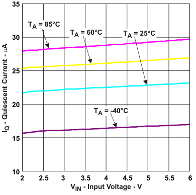
| IQ | Operating quiescent current | PFM operation (MODE = GND), IOUT = 0 mA, device not switching, TJ = –40°C to 85°C | 22 | 40 | μA | ||
| PFM operation (MODE = GND), IOUT = 0 mA, device switching, VOUT = 1.2 V | 25 | μA | |||||
| PWM operation (MODE = VIN), IOUT = 0 mA, device switching | 3 | mA | |||||
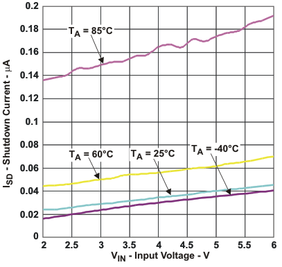
| ISD | Shutdown current | EN = GND, TJ = –40°C to 85°C | 0.1 | 1 | μA | ||
| VUVLO | Undervoltage lockout threshold | Falling | 1.8 | 1.9 | V | ||
| Rising | 1.9 | 2.05 | V | ||||
| ENABLE, MODE THRESHOLD | |||||||
| VIH TH | Threshold for detecting high EN, MODE | 2.05 V ≤ VIN ≤ 6 V , rising edge | 0.8 | 1 | V | ||
| VIL TH HYS | Threshold for detecting low EN, MODE | 2.05 V ≤ VIN ≤ 6 V , falling edge, TJ = –40°C to 85°C | 0.4 | 0.6 | V | ||
| Rpd | Pull-down resistor EN, MODE | TPS622319 | 1 | MΩ | |||
| IIN | Input bias current, EN, MODE | EN, MODE = GND or VIN, TJ = –40°C to 85°C, except TPS622319 | 0.01 | 0.5 | μA | ||
| POWER SWITCH | |||||||
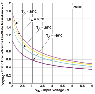
| RDS(ON) | High side MOSFET ON-resistance | VIN = 3.6 V, TJ = –40°C to 85°C | 600 | 850 | mΩ | ||
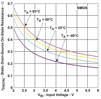
| Low Side MOSFET ON-resistance | 350 | 480 | |||||
| ILIMF | Forward current limit MOSFET high-side | VIN = 3.6 V, open-loop | 690 | 850 | 1050 | mA | |
| Forward current limit MOSFET low-side | 550 | 840 | 1220 | mA | |||
| TJSD | Thermal shutdown | Increasing junction temperature | 150 | °C | |||
| Thermal shutdown hysteresis | Decreasing junction temperature | 20 | °C | ||||
| CONTROLLER | |||||||
| tONmin | Minimum ON-time | MODE = VIN, IOUT = 0 mA | 135 | ns | |||
| tOFFmin | Minimum OFF-time | 40 | ns | ||||
| OUTPUT | |||||||
| VREF | Internal reference voltage | 0.7 | V | ||||
| VOUT | Output voltage accuracy(1) | MODE = GND, IOUT = 0 mA | 0% | ||||
| MODE = VIN, IOUT = 0 mA | TJ = 25°C | –2% | 2% | ||||
| TJ = –40°C to 125°C | –2.5% | 2.5% | |||||
| DC output voltage load regulation | MODE = VIN | 0.001 | %/mA | ||||
| DC output voltage line regulation | MODE = VIN, IOUT = 0 mA, 2.05 V ≤ VIN ≤ 6 V | 0 | %/V | ||||
| tStart | Start-up time | Time from active EN to VOUT = 1.8 V, 10-Ω load | 100 | μs | |||
| ILK_SW | Leakage current into SW pin | VIN = VOUT = VSW = 3.6 V, EN = GND(2) , TJ = –40°C to 85°C | 0.1 | 0.5 | μA | ||
(1) VIN = VO + 1.0 V
(2) The internal resistor divider network is disconnected from FB pin.
(3) In applications where high power dissipation and/or poor package thermal resistance is present, the maximum ambient temperature may have to be derated. Maximum ambient temperature (TA(max)) is dependent on the maximum operating junction temperature (TJ(max)), the maximum power dissipation of the device in the application (PD(max)), and the junction-to-ambient thermal resistance of the part/package in the application (RθJA), as given by the following equation: TA(max) = TJ(max) – (RθJA × PD(max)).
(4) The minimum required supply voltage for startup is 2.05 V. The part is functional down to the falling under voltage lockout (UVL) threshold.
7.6 Typical Characteristics


