ZHCSB84F November   2011  – November 2021 TPS62130 , TPS62130A , TPS62131 , TPS62132 , TPS62133

PRODUCTION DATA  

  1. 特性
  2. 应用
  3. 说明
  4. Revision History
  5. Device Comparison Table
  6. Pin Configuration and Functions
  7. Specifications
    1. 7.1 Absolute Maximum Ratings (1)
    2. 7.2 ESD Ratings
    3. 7.3 Recommended Operating Conditions
    4. 7.4 Thermal Information
    5. 7.5 Electrical Characteristics
    6. 7.6 Typical Characteristics
  8. Detailed Description
    1. 8.1 Overview
    2. 8.2 Functional Block Diagram
    3. 8.3 Feature Description
      1. 8.3.1 Enable / Shutdown (EN)
      2. 8.3.2 Soft Start / Tracking (SS/TR)
      3. 8.3.3 Power Good (PG)
      4. 8.3.4 Pin-Selectable Output Voltage (DEF)
      5. 8.3.5 Frequency Selection (FSW)
      6. 8.3.6 Undervoltage Lockout (UVLO)
      7. 8.3.7 Thermal Shutdown
    4. 8.4 Device Functional Modes
      1. 8.4.1 Pulse Width Modulation (PWM) Operation
      2. 8.4.2 Power Save Mode Operation
      3. 8.4.3 100% Duty-Cycle Operation
      4. 8.4.4 Current Limit And Short Circuit Protection
  9. Application and Implementation
    1. 9.1 Application Information
    2. 9.2 Typical Application
      1. 9.2.1 Design Requirements
      2. 9.2.2 Detailed Design Procedure
        1. 9.2.2.1 Programming The Output Voltage
        2. 9.2.2.2 External Component Selection
          1. 9.2.2.2.1 Inductor Selection
          2. 9.2.2.2.2 Capacitor Selection
            1. 9.2.2.2.2.1 Output Capacitor
            2. 9.2.2.2.2.2 Input Capacitor
            3. 9.2.2.2.2.3 Soft-Start Capacitor
        3. 9.2.2.3 Tracking Function
        4. 9.2.2.4 Output Filter And Loop Stability
      3. 9.2.3 Application Curves
    3. 9.3 System Examples
      1. 9.3.1 LED Power Supply
      2. 9.3.2 Active Output Discharge
      3. 9.3.3 –3.3-V Inverting Power Supply
      4. 9.3.4 Various Output Voltages
  10. 10Power Supply Recommendations
  11. 11Layout
    1. 11.1 Layout Guidelines
    2. 11.2 Layout Example
    3. 11.3 Thermal Information
  12. 12Device and Documentation Support
    1. 12.1 Device Support
      1. 12.1.1 第三方产品免责声明
    2. 12.2 Documentation Support
      1. 12.2.1 Related Documentation
    3. 12.3 接收文档更新通知
    4. 12.4 支持资源
    5. 12.5 Trademarks
    6. 12.6 Electrostatic Discharge Caution
    7. 12.7 术语表
  13. 13Mechanical, Packaging, and Orderable Information

封装选项

机械数据 (封装 | 引脚)
散热焊盘机械数据 (封装 | 引脚)
订购信息

–3.3-V Inverting Power Supply

The TPS62130 can be used as an inverting power supply by rearranging external circuitry as shown in Figure 9-42. As the former GND node now represents a voltage level below system ground, the voltage difference between VIN and VOUT has to be limited for operation to the maximum supply voltage of 17 V (see Equation 16).

Equation 16. GUID-55C6F539-0570-4E2E-99A2-0847E37F45D1-low.gif
GUID-D4378ACB-724E-4EA0-A9FF-9C816C48C195-low.gif
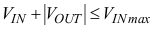
Figure 9-42 –3.3-V Inverting Power Supply

The transfer function of the inverting power supply configuration differs from the buck mode transfer function, incorporating a right half plane zero additionally. The loop stability has to be adapted and an output capacitance of at least 22 µF is recommended. A detailed design example is given in Using the TPS6215x in an Inverting Buck-Boost Topology Application Report.