ZHCSB84F November 2011 – November 2021 TPS62130 , TPS62130A , TPS62131 , TPS62132 , TPS62133
PRODUCTION DATA
- 1 特性
- 2 应用
- 3 说明
- 4 Revision History
- 5 Device Comparison Table
- 6 Pin Configuration and Functions
- 7 Specifications
- 8 Detailed Description
- 9 Application and Implementation
- 10Power Supply Recommendations
- 11Layout
- 12Device and Documentation Support
- 13Mechanical, Packaging, and Orderable Information
9.2.2.2.1 Inductor Selection
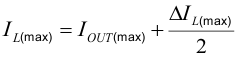
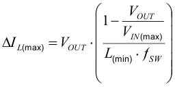
The inductor selection is affected by several effects like inductor ripple current, output ripple voltage, PWM-to-PSM transition point, and efficiency. In addition, the inductor selected has to be rated for appropriate saturation current and DC resistance (DCR). Equation 7 and Equation 8 calculate the maximum inductor current under static load conditions.
where
- IL(max) is the maximum inductor current.
- ΔIL is the peak-to-peak inductor ripple current.
- L(min) is the minimum effective inductor value.
- fSW is the actual PWM switching frequency.
Calculating the maximum inductor current using the actual operating conditions gives the required minimum saturation current of the inductor. It is recommended to add a margin of approximately 20%. A larger inductor value is also useful to get lower ripple current, but increases the transient response time and size as well. The following inductors have been used with the TPS6213x and are recommended for use:
| TYPE | INDUCTANCE [µH] | CURRENT [A](1) | DIMENSIONS [L × B × H] mm | MANUFACTURER(2) |
|---|---|---|---|---|
| XFL4020-102ME_ | 1.0 µH, ±20% | 4.7 | 4 × 4 × 2.1 | Coilcraft |
| XFL4020-152ME_ | 1.5 µH, ±20% | 4.2 | 4 × 4 × 2.1 | Coilcraft |
| XFL4020-222ME_ | 2.2 µH, ±20% | 3.8 | 4 × 4 × 2.1 | Coilcraft |
| IHLP1212BZ-11 | 1.0 µH, ±20% | 4.5 | 3 × 3.6 × 2 | Vishay |
| IHLP1212BZ-11 | 2.2 µH, ±20% | 3.0 | 3 × 3.6 × 2 | Vishay |
| SRP4020-3R3M | 3.3µH, ±20% | 3.3 | 4.8 × 4 × 2 | Bourns |
| VLC5045T-3R3N | 3.3µH, ±30% | 4.0 | 5 × 5 × 4.5 | TDK |
The inductor value also determines the load current at which power save mode is entered:
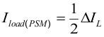
Using Equation 9, this current level can be adjusted by changing the inductor value.