ZHCSKG6 November 2019 TPS61391
PRODUCTION DATA.
- 1 特性
- 2 应用
- 3 说明
- 4 修订历史记录
- 5 Pin Configuration and Functions
- 6 Specifications
- 7 Detailed Description
-
8 Application and Implementation
- 8.1 Application Information
- 8.2
Typical Application
- 8.2.1 Design Requirement
- 8.2.2
Detailed Design Procedure
- 8.2.2.1 Selecting the Rectifier Diode
- 8.2.2.2 Selecting the Inductor
- 8.2.2.3 Selecting Output Capacitor
- 8.2.2.4 Selecting Filter Resistor and Capacitor
- 8.2.2.5 Setting the Output Voltage
- 8.2.2.6 Selecting Capacitor for CAP pin
- 8.2.2.7 Selecting Capacitor for AVCC pin
- 8.2.2.8 Selecting Capacitor for APD pin
- 8.2.2.9 Selecting the Resistors of MON1 or MON2
- 8.2.2.10 Selecting the Capacitors of MON1 or MON2
- 8.2.2.11 Selecting the Short Current Limit
- 8.2.3 Application Curves
- 9 Power Supply Recommendations
- 10Layout
- 11器件和文档支持
- 12机械、封装和可订购信息
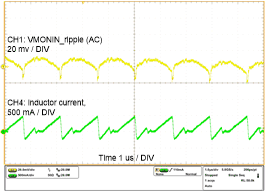
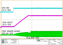
8.2.3 Application Curves
Typical condition VIN = 3.3 V, VOUT = 60 V, RSHORT = 5 kΩ, RMON1/2 = 3.01 kΩ and CMON1/2 = 10 pF.
Application waveforms are measured with the inductor 4.7 µH and the output capacitance 0.1 µF at room temperature.

| VIN = 3.3 V | VOUT = 60 V | APD current = 1 mA |

| VIN = 3.3 V | VOUT = 60 V | APD current = 1mA |