ZHCSID4B June 2018 – January 2021 TPS61372
PRODUCTION DATA
- 1 特性
- 2 应用
- 3 说明
- 4 Revision History
- 5 Pin Configuration and Functions
- 6 Specifications
- 7 Detailed Description
-
8 Application and Implementation
- 8.1 Application Information
- 8.2
Typical Application
- 8.2.1 Design Requirements
- 8.2.2
Detailed Design Procedure
- 8.2.2.1 Custom Design With WEBENCH® Tools
- 8.2.2.2 Setting the Output Voltage
- 8.2.2.3 Selecting the Inductor
- 8.2.2.4 Selecting the Output Capacitors
- 8.2.2.5 Selecting the Input Capacitors
- 8.2.2.6 Loop Stability and Compensation
- 8.2.2.7 Loop Compensation Design Steps
- 8.2.2.8 Selecting the Bootstrap Capacitor
- 8.2.3 Application Curves
- 9 Power Supply Recommendations
- 10Layout
- 11Device and Documentation Support
- 12Mechanical, Packaging, and Orderable Information
8.2.2.7 Loop Compensation Design Steps
With the small signal models coming out, the next step is to calculate the compensation network parameters with the given inductor and output capacitance.
- Set the Crossover Frequency, ƒC.
- The first step is to set the loop crossover frequency, ƒC. The higher crossover frequency, the faster the loop response is. It is generally accepted that the loop gain cross over no higher than the lower of either 1/10 of the switching frequency, ƒSW, or 1/5 of the RHPZ frequency, ƒRHPZ. Then calculate the loop compensation network values of Rc, Cc, and Cp in following sections.
- Set the Compensation Resistor, RC.
- By placing ƒZ below ƒC, for frequencies above ƒC, RC | | REA approximately = RC, so RC × GEA sets the compensation gain. Setting the compensation gain, KCOMP-dB, at ƒZ, results in the total loop gain, T(s) = GPS(s) × HEA(s) × He(s) being zero at ƒC.
- Therefore, to approximate a single-pole rolloff
up to fP2, rearrange Equation 19 to solve for RC so that the compensation gain, KEA, at
fC is the negative of the gain, KPS, read at
frequency fC for the power stage bode plot or more simply:
Equation 19.
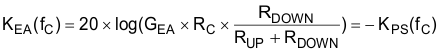
where
- KEA is gain of the error amplifier network
- KPS is the gain of the power stage
- GEA is the transconductance of the amplifier, the typical value of GEA = 175 µA / V
- Set the compensation zero capacitor, CC.
- Place the compensation zero at the power stage
pole position of ROUT, COUT to get:
Equation 20.
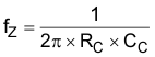
- Set ƒZ = ƒP, and get:
Equation 21.
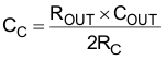
- Place the compensation zero at the power stage
pole position of ROUT, COUT to get:
- Set the compensation pole capacitor, CP.
- Place the compensation pole at the zero produced
by the RESR and the COUT. It is useful for
canceling unhelpful effects of the ESR zero. Equation 22.
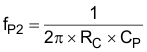 Equation 23.
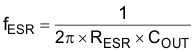
- Set ƒP2 = ƒESR, and get:
Equation 24.
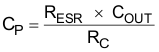
- If the calculated value of CP is less than 10 pF, it can be neglected.
- Place the compensation pole at the zero produced
by the RESR and the COUT. It is useful for
canceling unhelpful effects of the ESR zero.