ZHCSCS7A September   2014  – September 2014 TPS61291

PRODUCTION DATA.  

  1. 特性
  2. 应用
  3. 说明
  4. 修订历史记录
  5. Pin Configuration and Functions
  6. Specifications
    1. 6.1 Absolute Maximum Ratings
    2. 6.2 Handling Ratings
    3. 6.3 Recommended Operating Conditions
    4. 6.4 Thermal Information
    5. 6.5 Electrical Characteristics
    6. 6.6 Typical Characteristics
  7. Detailed Description
    1. 7.1 Overview
    2. 7.2 Functional Block Diagram
    3. 7.3 Feature Description
      1. 7.3.1 Bypass / Boost Mode Operation EN/BYP
      2. 7.3.2 Output Voltage Selection VSEL
      3. 7.3.3 Feedback Divider Disconnect
      4. 7.3.4 Undervoltage Lockout
      5. 7.3.5 Overtemperature Protection
      6. 7.3.6 Overvoltage Protection
    4. 7.4 Device Functional Modes
      1. 7.4.1 Boost Mode Operation
      2. 7.4.2 Bypass Mode Operation
      3. 7.4.3 Controlled Transition into Bypass Mode
      4. 7.4.4 Operation at Output Overload
      5. 7.4.5 Startup
  8. Applications and Implementation
    1. 8.1 Application Information
    2. 8.2 Typical Application
      1. 8.2.1 Design Requirements
      2. 8.2.2 Detailed Design Procedure
        1. 8.2.2.1 Inductor Selection
        2. 8.2.2.2 Input and Output Capacitor Selection
      3. 8.2.3 Application Curves
  9. Power Supply Recommendations
  10. 10Layout
    1. 10.1 Layout Guidelines
    2. 10.2 Layout Example
  11. 11器件和文档支持
    1. 11.1 器件支持
      1. 11.1.1 第三方产品免责声明
    2. 11.2 文档支持
      1. 11.2.1 相关文档 
    3. 11.3 商标
    4. 11.4 静电放电警告
    5. 11.5 术语表
  12. 12机械封装和可订购信息

封装选项

机械数据 (封装 | 引脚)
散热焊盘机械数据 (封装 | 引脚)
订购信息

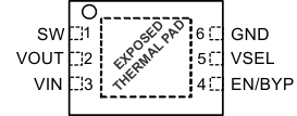
5 Pin Configuration and Functions

DRV Package
6 Pin
Top View
po_TPS61290.gif

Pin Functions

PIN I/O DESCRIPTION
NAME NO.
SW 1 I Switch node of the converter. Connect the inductor between this pin and the input capacitor CIN.
VOUT 2 O Boost converter output. Connect the output capacitor COUT between this pin and GND close to the device.
VIN 3 PWR Input voltage supply pin for the boost converter. Connect the input capacitor CIN between this pin and GND as close as possible to the device.
EN/BYP 4 I Control pin of the device. A high level enables the boost mode operation. A low level disables the boost converter and enables bypass mode operation. EN/BYP must be actively terminated high or low. Usually, this pin is controlled by the MCU in the system.
VSEL 5 I Output voltage selection pin. The logic level of this pin is read out during startup and internally latched. Connect this pin only to GND, VOUT, or leave it floating.
GND 6 PWR Ground pin of the device.
EXPOSED THERMAL PAD NC Not electrically connected to the IC, but must be soldered to achieve specified thermal performance. Connect this pad to the GND pin and use it as a central GND plane.