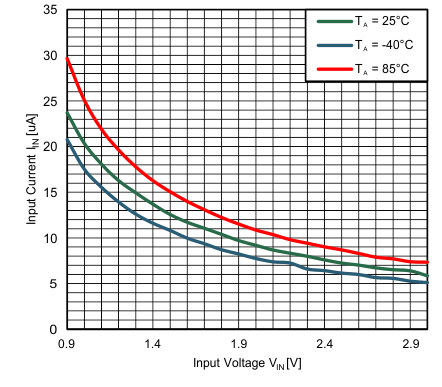
8.2.1 Design Requirements
The TPS61291 is a highly integrated boost converter. The output voltage is set internally via a VSEL pin without any additional components. For operation, only an input capacitor, output capacitor, and an inductor are required. Table 1 shows the components used for the application characteristic curves.
Table 1. Components for Application Characteristic Curves(1)
| Reference |
Description |
Value |
Manufacturer |
|
| TPS61291 |
Low Iq Boost Converter with Bypass Operation |
|
Texas Instruments |
|
| CIN |
Input capacitor |
10µF |
Murata |
GRM219R61A106KE44D |
| COUT |
Output capacitor |
22µF |
Murata |
GRM21BR60J226ME39L |
| L |
Inductor |
3.3µH |
Coilcraft |
LPS3314 3R3 |
(1) See the Third-Party Products Disclaimer in the
Device Support section.
8.2.2 Detailed Design Procedure
The external components have to fulfill the needs of the application but also the stability criteria of the device's control loop. The TPS61291 is optimized to work within a range of L and C combinations. The LC output filter inductance and capacitance must be considered together. The output capacitor sets the corner frequency of the converter while the inductor creates a Right-Half-Plane-Zero degrading the stability of the converter. Consequently with a larger inductor a bigger capacitor has to be used to guarantee a stable loop. Table 2 shows the output filter component selection.
Table 2. Recommended LC Output Filter Combinations
| Output voltage [V] |
Inductor value [µH](2) |
Output capacitor value [µF](1) |
| 22 |
22 + 10 |
2 x 22 |
| 3.3 / 3.0 |
3.3 |
√(3) |
√ |
√ |
| 4.7 |
|
|
√ |
| 2.5 |
2.2 |
√ |
√ |
√ |
| 3.3 |
|
√(3) |
√ |
(1) Capacitance tolerance and bias voltage de-rating is anticipated. The effective capacitance can vary by 20% and -50%.
(2) Inductor tolerance and current de-rating is anticipated. The effective inductance can vary by 20% and -30%.
(3) This LC combination is the standard value and recommended for most applications.
8.2.2.1 Inductor Selection
The device is optimized to operate with a 3.3µH inductor value. Other inductor values can be used, per Table 2. The maximum inductor current can be approximated by the ILMAX, from Equation 1. For proper operation, the inductor needs to be rated for a saturation current which is higher than the switch current limit of typically 1A. Table 3 lists inductors that have been tested with the TPS61291.
Equation 1.
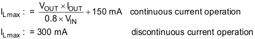
Table 3. List of Inductors(1)
| INDUCTANCE |
DIMENSIONS [mm3] |
TYPE |
SUPPLIER |
| 3.3 |
3.3 x 3.3 x 1.3 |
LPS3314 |
Coilcraft |
| 3.3 |
2.95 x 2.95 x 1.4 |
LPS3015 |
| 3.3 |
3 x 2.5 x 1.5 |
VLF302515 |
TDK |
| 3.3 |
2 x 2 x 1.2 |
MDMK2020T3R3M |
Taiyo Yuden |
| 3.3 |
2.5 x 2.0 x 1.2 |
DFE252012 |
Toko |
| 3.3 |
3.0 x 3.0 x 1.5 |
74438335033 |
Würth |
(1) See the Third-Party Products Disclaimer in the
Device Support section.
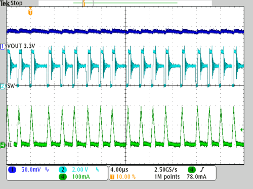
8.2.2.2 Input and Output Capacitor Selection
For best output and input voltage filtering, low ESR X5R or X7R ceramic capacitors are recommended. The input capacitor minimizes input voltage ripple, suppresses input voltage spikes and provides a stable system rail for the device. At least a 10μF or larger input capacitor is recommended for operation. In applications in which the power source (e.g. certain battery chemistries) shows an internal resistance characteristic, a larger input capacitor might be used to buffer the supply voltage for the TPS61291. The recommended typical output capacitor value is 22 μF and can vary as outlined in the output filter selection Table 2.
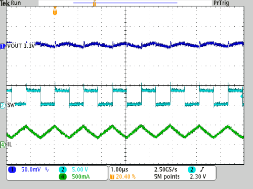
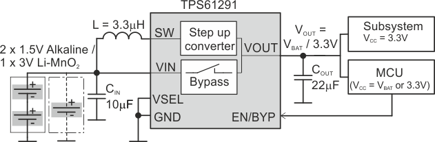 Figure 8. Typical Application Circuit with Regulated 3.3V VOUT / VBAT
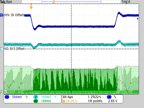
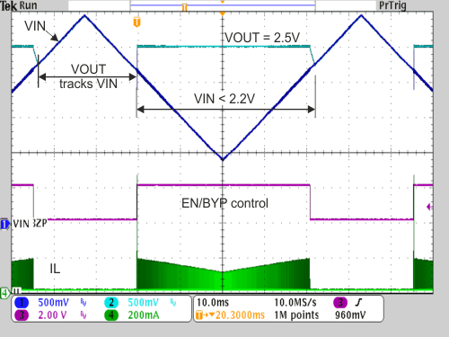
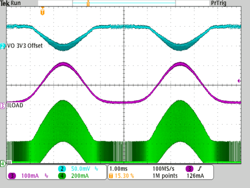
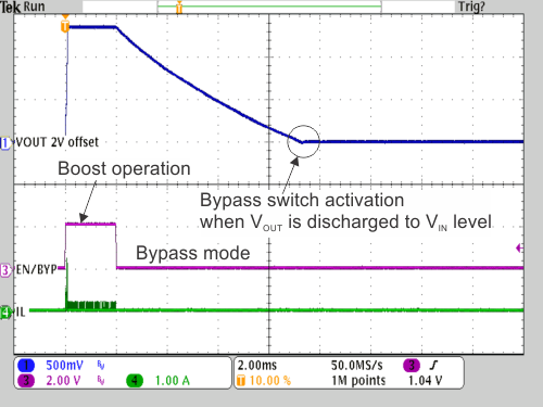
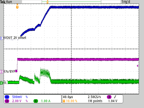
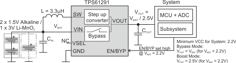 Figure 9. Bypass Mode / Boost Mode Operation to Maintain Sufficient System Voltage