ZHCSGX8E march 2017 – june 2023 TPS61253A , TPS61253E
PRODUCTION DATA
- 1
- 1 特性
- 2 应用
- 3 说明
- 4 Revision History
- 5 Device Comparison
- 6 Pin Configuration and Functions
- 7 Specifications
- 8 Detailed Description
- 9 Application and Implementation
- Power Supply Recommendations
- 10Layout
- 11Device and Documentation Support
- Mechanical, Packaging, and Orderable Information
8.3.4 Current Limit Operation
During the start-up phase, the output current is limited to the pre-charge current limit which is specified as the ILIM_DC in Section 7.5.
The TPS61253x employs a valley current sensing scheme at the normal boost switching phase. When the output load is increased, the cycle-by-cycle valley current limit will be triggered. As shown in Figure 8-1, the maximum continuous output current, prior to entering the current limit operation, can be defined by Equation 1:
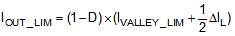


where
- IOUT_LIM is the output current limit, IVALLEY_LIM is switching valley current limit
- ΔIL is the peak-peak inductor current ripple
- D is the duty cycle, f is the switching frequency, η is the efficiency, L is the inductor
- VOUT is the output voltage, VIN is the input voltage
 Figure 8-1 Current Limit Operation
If the output current is further increased and triggers the short protection threshold (typical 6 A of inductor current), the TPS61253x enters into hiccup mode. Once the hiccup is triggered, the device turns on the high-side FET for around 1 ms with the pre-charge current limit and stops for around 20 ms. The hiccup on / off cycle repeats again and again if the short condition is present. Figure 8-2 illustrates the TPS61253x working scheme of the hiccup mode. The average current and thermal will be much lowered at the hiccup steady state and the device can recover automatically as long as the short releases.
 Figure 8-2 Hiccup Mode Short Protection