ZHCSJM5D September 2009 – April 2019 TPS61093
PRODUCTION DATA.
- 1 特性
- 2 应用
- 3 说明
- 4 修订历史记录
- 5 Pin Configuration and Functions
- 6 Specifications
- 7 Detailed Description
- 8 Application and Implementation
- 9 Power Supply Recommendations
- 10Layout
- 11器件和文档支持
- 12机械、封装和可订购信息
8.2.1.2.8 Small Signal Stability
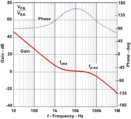
The TPS61093 integrates slope compensation and the RC compensation network for the internal error amplifier. Most applications are control loop stable if the recommended inductor and input/output capacitors are used. For those few applications that require components outside the recommended values, the internal error amplifier’s gain and phase are presented in Figure 9.
 Figure 9. Bode Plot of Error Amplifier Gain and Phase
 The RC compensation network generates a pole fp-ea of 57 kHz and a zero fz-ea of 1.9 kHz, shown in Figure 9. Use Equation 7 to calculate the output pole, fP, of the boost converter. If fP << fz-ea. due to a large capacitor beyond 10 μF, for example, a feed forward capacitor on the resistor divider, as shown in Figure 9, is necessary to generate an additional zero fz-f. to improve the loop phase margin and improve the load transient response. The low frequency pole fp-f and zero fz-f generated by the feed forward capacitor are given by Equation 8 and Equation 9:


where
- Cff = the feed-forward capacitor
For example, in the typical application circuitry (see Figure 7), the output pole fP is approximately 1 kHz. When the output capacitor is increased to 100 μF, then the fP is reduced to 10 Hz. Therefore, a feed-forward capacitor of 10 nF compensates for the low frequency pole.
A feed-forward capacitor that sets fz-f near 10 kHz improves the load transient response in most applications, as shown in Figure 11.