SLVS859B June 2008 – December 2014 TPS61085
PRODUCTION DATA.
- 1 Features
- 2 Applications
- 3 Description
- 4 Simplified Schematic
- 5 Revision History
- 6 Pin Configuration and Functions
- 7 Specifications
- 8 Detailed Description
- 9 Application and Implementation
- 10Power Supply Recommendations
- 11Layout
- 12Device and Documentation Support
- 13Mechanical, Packaging, and Orderable Information
11 Layout
11.1 Layout Guidelines
For all switching power supplies, the layout is an important step in the design, especially at high peak currents and high switching frequencies. If the layout is not carefully done, the regulator could show stability problems as well as EMI problems. Therefore, use wide and short traces for the main current path and for the power ground tracks. The input capacitor, output capacitor, and the inductor should be placed as close as possible to the IC. Use a common ground node for power ground and a different one for control ground to minimize the effects of ground noise. Connect these ground nodes at the GND terminal of the IC. The most critical current path for all boost converters is from the switching FET, through the rectifier diode, then the output capacitors, and back to ground of the switching FET. Therefore, the output capacitors and their traces should be placed on the same board layer as the IC and as close as possible between the IC’s SW and GND terminal.
11.2 Layout Example
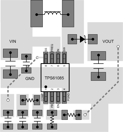 Figure 22. TPS61085 Layout Example