SLVS859B June 2008 – December 2014 TPS61085
PRODUCTION DATA.
- 1 Features
- 2 Applications
- 3 Description
- 4 Simplified Schematic
- 5 Revision History
- 6 Pin Configuration and Functions
- 7 Specifications
- 8 Detailed Description
- 9 Application and Implementation
- 10Power Supply Recommendations
- 11Layout
- 12Device and Documentation Support
- 13Mechanical, Packaging, and Orderable Information
8 Detailed Description
8.1 Overview
The boost converter is designed for output voltages up to 18.5 V with a switch peak current limit of 2.0 A minimum. The device, which operates in a current mode scheme with quasi-constant frequency, is externally compensated for maximum flexibility and stability. The switching frequency is selectable between 650 kHz and 1.2 MHz and the minimum input voltage is 2.3 V. To control the inrush current at start-up a soft-start pin is available.
TPS61085 boost converter’s novel topology using adaptive off-time provides superior load and line transient responses and operates also over a wider range of applications than conventional converters.
The selectable switching frequency offers the possibility to optimize the design either for the use of small sized components (1.2 MHz) or for higher system efficiency (650 kHz). However, the frequency changes slightly because the voltage drop across the rDS(on) has some influence on the current and voltage measurement and thus on the on-time (the off-time remains constant).
The converter operates in continuous conduction mode (CCM) as soon as the input current increases above half the ripple current in the inductor, for lower load currents it switches into discontinuous conduction mode (DCM). If the load is further reduced, the part starts to skip pulses to maintain the output voltage.
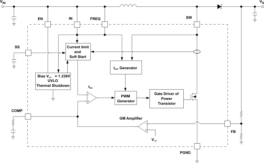
8.2 Functional Block Diagram
8.3 Feature Description
8.3.1 Soft-Start
The boost converter has an adjustable soft-start to prevent high inrush current during start-up. To minimize the inrush current during start-up an external capacitor connected to the soft-start pin SS and charged with a constant current, is used to slowly ramp up the internal current limit of the boost converter when charged with a constant current. When the EN pin is pulled high, the soft-start capacitor CSS is immediately charged to 0.3 V. The capacitor is then charged at a constant current of 10 μA typically until the output of the boost converter VS has reached its Power Good threshold (roughly 98% of VS nominal value). During this time, the SS voltage directly controls the peak inductor current, starting with 0 A at VSS = 0.3 V up to the full current limit at VSS =0.8 V. The maximum load current is available after the soft-start is completed. The larger the capacitor the slower the ramp of the current limit and the longer the soft-start time. A 100 nF capacitor is usually sufficient for most of the applications. When the EN pin is pulled low, the soft-start capacitor is discharged to ground.
8.3.2 Frequency Select Pin (FREQ)
The frequency select pin FREQ allows to set the switching frequency of the device to 650 kHz (FREQ = low) or 1.2 MHz (FREQ = high). Higher switching frequency improves load transient response but reduces slightly the efficiency. The other benefits of higher switching frequency are a lower output ripple voltage. The use of the 1.2 MHz switching frequency is recommended unless light load efficiency is a major concern.
8.3.3 Undervoltage Lockout (UVLO)
To avoid mis-operation of the device at low input voltages an undervoltage lockout is included that disables the device, if the input voltage falls below 2.2 V.
8.3.4 Thermal Shutdown
A thermal shutdown is implemented to prevent damages due to excessive heat and power dissipation. Typically the thermal shutdown threshold happens at a junction temperature of 150°C. When the thermal shutdown is triggered the device stops switching until the temperature falls below typically 136°C. Then the device starts switching again.
8.3.5 Overvoltage Prevention
If overvoltage is detected on the FB pin (typically 3 % above the nominal value of 1.238 V) the part stops switching immediately until the voltage on this pin drops to its nominal value. This prevents overvoltage on the output and secures the circuits connected to the output from excessive overvoltage.
8.4 Device Functional Modes
The converter operates in continuous conduction mode (CCM) as soon as the input current increases above half the ripple current in the inductor, for lower load currents it switches into discontinuous conduction mode (DCM). If the load is further reduced, the part starts to skip pulses to maintain the output voltage.