ZHCSJ97B September   2009  – January 2019 TPS60151

PRODUCTION DATA.  

  1. 特性
  2. 应用
  3. 说明
    1.     Device Images
      1.      典型应用原理图
      2.      效率与输入电压间的关系
  4. 修订历史记录
  5. Device Comparison Table
  6. Pin Configuration and Functions
    1.     Pin Functions
  7. Specifications
    1. 7.1 Absolute Maximum Ratings
    2. 7.2 ESD Ratings
    3. 7.3 Recommended Operating Conditions
    4. 7.4 Thermal Information
    5. 7.5 Electrical Characteristics
    6. 7.6 Typical Characteristics
  8. Detailed Description
    1. 8.1 Overview
    2. 8.2 Functional Block Diagram
    3. 8.3 Feature Description
      1. 8.3.1 Enable
      2. 8.3.2 Output Reverse Current Protection
      3. 8.3.3 Undervoltage Lockout
      4. 8.3.4 Thermal Shutdown Protection
    4. 8.4 Device Functional Modes
      1. 8.4.1 Soft Start
      2. 8.4.2 Normal Mode and Skip Mode Operation
      3. 8.4.3 Over-current Protection and Short-Circuit Protection
  9. Application and Implementation
    1. 9.1 Application Information
    2. 9.2 Typical Application
      1. 9.2.1 Design Requirements
      2. 9.2.2 Detailed Design Procedure
        1. 9.2.2.1 Capacitor Selection
      3. 9.2.3 Application Curves
    3. 9.3 System Example
      1. 9.3.1 Circuit for Driving White LEDs
  10. 10Power Supply Recommendations
  11. 11Layout
    1. 11.1 Layout Guidelines
    2. 11.2 Layout Example
  12. 12器件和文档支持
    1. 12.1 接收文档更新通知
    2. 12.2 社区资源
    3. 12.3 商标
    4. 12.4 静电放电警告
    5. 12.5 术语表
  13. 13机械、封装和可订购信息

封装选项

机械数据 (封装 | 引脚)
散热焊盘机械数据 (封装 | 引脚)
订购信息

Overview

The TPS60151, regulated charge pump, provides a regulated output voltage for various input voltages. The TPS60151 regulates the voltage across the flying capacitor to 2.5 V and controls the voltage drop of Q1 and Q2 while a conversion clock with 50% duty cycle drives the FETs.
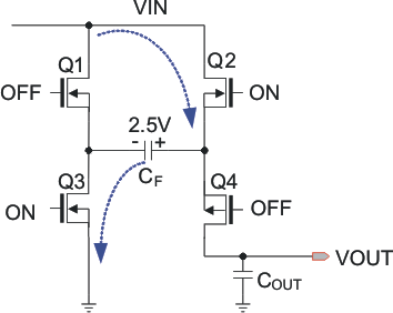
TPS60151 chg_mode_lvs888.gifFigure 3. Charging Mode

During the first half cycle, Q2 and Q3 transistors are turned on and flying capacitor, CF, will be charged to 2.5 V ideally.
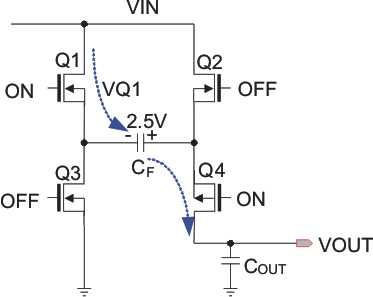
TPS60151 dischg_mode_lvs888.gifFigure 4. Discharging Mode

During the second half cycle, Q1 and Q4 transistors are turned on. Capacitor CF will then be discharged to output.

The output voltage can be calculated as follows:

Equation 1. Vout = VIN – VQ1 + V(CF) - VQ4 = VIN – VQ1 + 2.5 V - VQ4 = 5 V. (Ideal)

The output voltage is regulated by output feedback and an internally compensated voltage control loop.