ZHCSJ24A November 2018 – May 2019 TPS56339
PRODUCTION DATA.
- 1 特性
- 2 应用
- 3 说明
- 4 修订历史记录
- 5 Pin Configuration and Functions
- 6 Specifications
-
7 Detailed Description
- 7.1 Overview
- 7.2 Functional Block Diagram
- 7.3
Feature Description
- 7.3.1 Advanced Emulated Current Mode Control
- 7.3.2 Enable and Adjusting Undervoltage Lockout
- 7.3.3 Soft Start and Pre-Biased Soft Start
- 7.3.4 Voltage Reference
- 7.3.5 Minimum ON-time, Minimum OFF-time and Frequency Foldback at Dropout Conditions
- 7.3.6 Overcurrent and Undervoltage Protection
- 7.3.7 Thermal Shutdown
- 7.4 Device Functional Modes
- 7.5 Light-Load Operation
- 8 Application and Implementation
- 9 Power Supply Recommendations
- 10Layout
- 11器件和文档支持
- 12机械、封装和可订购信息
5 Pin Configuration and Functions
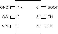
DDC Package
6-Pin SOT
Top View

Pin Functions
| PIN | I/O(1) | DESCRIPTION | |
|---|---|---|---|
| NAME | NO. | ||
| BOOT | 6 | O | A 30-Ω boot resistor and a 0.1-μF bootstrap cap are required between BOOT and SW. The voltage on this cap carries the gate drive voltage for the high-side MOSFET. |
| EN | 5 | I | Enable pin. Float to enable. Adjust the input undervoltage lockout with two resistors. |
| FB | 4 | I | Converter feedback input. Connect to output voltage with feedback resistor divider. |
| GND | 1 | G | Ground pin. Source terminal of low-side MOSFET as well as the ground terminal for controller circuit. Connect sensitive FB to this GND at a single point. |
| SW | 2 | O | Switch node connection between high-side MOSFET and low-side MOSFET. |
| VIN | 3 | I | Input voltage supply pin. The drain terminal of high-side MOSFET. |
(1) I = Input, O = Output, G = GND