ZHCSJ24A November 2018 – May 2019 TPS56339
PRODUCTION DATA.
- 1 特性
- 2 应用
- 3 说明
- 4 修订历史记录
- 5 Pin Configuration and Functions
- 6 Specifications
-
7 Detailed Description
- 7.1 Overview
- 7.2 Functional Block Diagram
- 7.3
Feature Description
- 7.3.1 Advanced Emulated Current Mode Control
- 7.3.2 Enable and Adjusting Undervoltage Lockout
- 7.3.3 Soft Start and Pre-Biased Soft Start
- 7.3.4 Voltage Reference
- 7.3.5 Minimum ON-time, Minimum OFF-time and Frequency Foldback at Dropout Conditions
- 7.3.6 Overcurrent and Undervoltage Protection
- 7.3.7 Thermal Shutdown
- 7.4 Device Functional Modes
- 7.5 Light-Load Operation
- 8 Application and Implementation
- 9 Power Supply Recommendations
- 10Layout
- 11器件和文档支持
- 12机械、封装和可订购信息
7.3.5 Minimum ON-time, Minimum OFF-time and Frequency Foldback at Dropout Conditions
Minimum ON-time, TON_MIN, is the smallest duration of time that the high-side MOSFET can be on. TON_MIN is typically 55ns in the TPS56339. Minimum OFF-time, TOFF_MIN, is the smallest duration that the high-side MOSFET can be off. TOFF_MIN is typically 115 ns in the TPS56339. In CCM operation, TON_MIN and TOFF_MIN limit the voltage conversion range given a fixed switching frequency.
The minimum duty cycle allowed is:
And the maximum duty cycle allowed is:
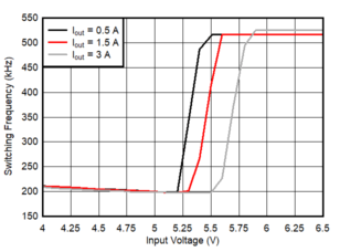
In the TPS56339, a frequency foldback scheme is employed to extend the maximum duty cycle when TOFF_MIN is reached. The switching frequency decreases once longer duty cycle is needed under low VIN conditions. With the duty increase, the on time will increase, until up to the Maximum ON-time, 5 μs. Wide range of frequency foldback allows the TPS56339 output voltage stay in regulation with a much lower supply voltage VIN. This leads to a lower effective dropout voltage.
Given an output voltage, the maximum operation supply voltage can be found by:

At lower supply voltage, the switching frequency decreases once TOFF_MIN is triggered. The minimum VIN without frequency foldback can be approximated by:

Taking considerations of power losses in the system with heavy load operation, VIN_MAX is higher than the result calculated in Equation 6. With frequency foldback, VIN_MIN is lowered by decreased fSW, as shown in Figure 16 .
 Figure 16. Frequency Foldback at Dropout (VOUT = 5 V)