ZHCSMV4A December 2020 – December 2022 TPS548B28
PRODUCTION DATA
- 1 特性
- 2 应用
- 3 说明
- 4 Revision History
- 5 Pin Configuration and Functions
- 6 Specifications
-
7 Detailed Description
- 7.1 Overview
- 7.2 Functional Block Diagram
- 7.3
Feature Description
- 7.3.1 Internal VCC LDO And Using External Bias On VCC Pin
- 7.3.2 Enable
- 7.3.3 Output Voltage Setting
- 7.3.4 Internal Fixed Soft Start and External Adjustable Soft Start
- 7.3.5 External REFIN For Output Voltage Tracking
- 7.3.6 Frequency and Operation Mode Selection
- 7.3.7 D-CAP3™ Control Mode
- 7.3.8 Low-side FET Zero-Crossing
- 7.3.9 Current Sense and Positive Overcurrent Protection
- 7.3.10 Low-side FET Negative Current Limit
- 7.3.11 Power Good
- 7.3.12 Overvoltage and Undervoltage Protection
- 7.3.13 Out-Of-Bounds (OOB) Operation
- 7.3.14 Output Voltage Discharge
- 7.3.15 UVLO Protection
- 7.3.16 Thermal Shutdown
- 7.4 Device Functional Modes
-
8 Application and Implementation
- 8.1 Application Information
- 8.2
Typical Application
- 8.2.1 Design Requirements
- 8.2.2
Detailed Design Procedure
- 8.2.2.1 Output Voltage Setting Point
- 8.2.2.2 Choose the Switching Frequency and the Operation Mode
- 8.2.2.3 Choose the Inductor
- 8.2.2.4 Set the Current Limit (TRIP)
- 8.2.2.5 Choose the Output Capacitor
- 8.2.2.6 Choose the Input Capacitors (CIN)
- 8.2.2.7 Soft Start Capacitor (SS/REFIN Pin)
- 8.2.2.8 EN Pin Resistor Divider
- 8.2.2.9 VCC Bypass Capacitor
- 8.2.2.10 BOOT Capacitor
- 8.2.2.11 PGOOD Pullup Resistor
- 8.2.3 Application Curves
- 8.3 Power Supply Recommendations
- 8.4 Layout
- 9 Device and Documentation Support
- 10Mechanical, Packaging, and Orderable Information
8.2.2.8 EN Pin Resistor Divider
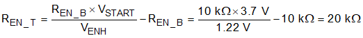
A resistor divider on the EN pin can be used to increase the input voltage the converter begins its start-up sequence. To set the start voltage, first select the bottom resistor (REN_B). The recommended value is between 1 kΩ and 100 kΩ. There is an internal pulldown resistance with a nominal value of 6 MΩ, which must be included for the most accurate calculations. This is especially important when the bottom resistor is a higher value, near 100 kΩ. This example uses a 10-kΩ resistor and combined with the internal resistance in parallel results in an equivalent bottom resistance of 9.98 kΩ. The top resistor value for the target start voltage is calculated with Equation 28. In this example, the nearest standard value of 20 kΩ is selected for REN_T. When selecting a start voltage in a wide input range application, be cautious that the EN pin absolute maximum voltage of 6 V is not exceeded.
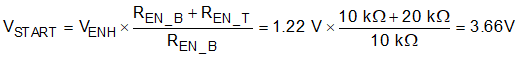
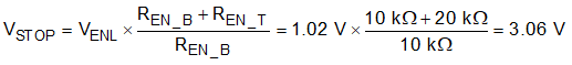
The start and stop voltages with the selected EN resistor divider can be calculated with Equation 29 and Equation 30.