ZHCS924D May   2012  – April 2021 TPS54526

PRODUCTION DATA  

  1. 特性
  2. 应用
  3. 说明
  4. Revision History
  5. Pin Configuration and Functions
  6. Specifications
    1. 6.1 Absolute Maximum Ratings
    2. 6.2 Handling Ratings
    3. 6.3 Recommended Operating Conditions
    4. 6.4 Thermal Information
    5. 6.5 Electrical Characteristics
    6. 6.6 Timing Requirements
    7. 6.7 Typical Characteristics
  7. Detailed Description
    1. 7.1 Overview
    2. 7.2 Functional Block Diagram
    3. 7.3 Feature Description
      1. 7.3.1  PWM Operation
      2. 7.3.2  PWM Frequency and Adaptive On-Time Control
      3. 7.3.3  Soft Start and Pre-Biased Soft Start
      4. 7.3.4  Power Good
      5. 7.3.5  VREG5
      6. 7.3.6  Output Discharge Control
      7. 7.3.7  Current Protection
      8. 7.3.8  Over/Under Voltage Protection
      9. 7.3.9  UVLO Protection
      10. 7.3.10 Thermal Shutdown
    4. 7.4 Device Functional Modes
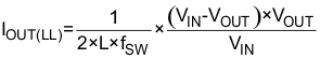
      1. 7.4.1 Auto-Skip Eco-Mode™ Control
  8. Application and Implementation
    1. 8.1 Application Information
    2. 8.2 Typical Application
      1. 8.2.1 Design Requirements
      2. 8.2.2 Detailed Design Procedure
        1. 8.2.2.1 Step By Step Design Procedure
        2. 8.2.2.2 Output Voltage Resistors Selection
        3. 8.2.2.3 Output Filter Selection
        4. 8.2.2.4 Input Capacitor Selection
        5. 8.2.2.5 Bootstrap Capacitor Selection
        6. 8.2.2.6 VREG5 Capacitor Selection
      3. 8.2.3 Application Curve
  9. Power Supply Recommendations
  10. 10Layout
    1. 10.1 Layout Guidelines
    2. 10.2 Layout Example
  11. 11Device and Documentation Support
    1. 11.1 接收文档更新通知
    2. 11.2 支持资源
    3. 11.3 Trademarks
    4. 11.4 静电放电警告
    5. 11.5 术语表
  12. 12Mechanical, Packaging, and Orderable Information
    1. 12.1 Thermal Information

封装选项

机械数据 (封装 | 引脚)
散热焊盘机械数据 (封装 | 引脚)
订购信息

Auto-Skip Eco-Mode™ Control

The TPS54526 is designed with Auto-Skip Eco-mode™ to increase light load efficiency. As the output current decreases from heavy load condition, the inductor current is also reduced and eventually comes to point that its rippled valley touches zero level, which is the boundary between continuous conduction and discontinuous conduction modes. The rectifying MOSFET is turned off when its zero inductor current is detected. As the load current further decreases the converter run into discontinuous conduction mode. The on-time is kept almost the same as it was in the continuous conduction mode so that it takes longer time to discharge the output capacitor with smaller load current to the level of the reference voltage. The transition point to the light load operation IOUT(LL) current can be calculated in Equation 2.

Equation 2. GUID-109DD237-FE25-4C93-94CE-F7FA65DE3B37-low.gif