ZHCSCI5B May 2014 – July 2016 TPS544B20 , TPS544C20
PRODUCTION DATA.
- 1 特性
- 2 应用范围
- 3 说明
- 4 修订历史记录
- 5 Device Comparison Table
- 6 Pin Configuration and Functions
- 7 Specifications
-
8 Detailed Description
- 8.1 Overview
- 8.2 Functional Block Diagram
- 8.3
Feature Description
- 8.3.1 Turn-On and Turn-Off Delay and Sequencing
- 8.3.2 Pre-Biased Output Start-Up
- 8.3.3 Voltage Reference
- 8.3.4 Differential Remote Sense and Output Voltage Setting
- 8.3.5 PMBus Output Voltage Adjustment
- 8.3.6 Switching Frequency
- 8.3.7 Soft-Start
- 8.3.8 Linear Regulators BP3 and BP6
- 8.3.9 External Bypass (BPEXT)
- 8.3.10 Current Monitoring and Low-Side MOSFET Overcurrent Protection
- 8.3.11 High-Side MOSFET Short-Circuit Protection
- 8.3.12 Over-Temperature Protection
- 8.3.13 Input Undervoltage Lockout (UVLO)
- 8.3.14 Output Overvoltage and Undervoltage Protection
- 8.3.15 Fault Protection Responses
- 8.3.16 PMBus General Description
- 8.3.17 PMBus Address
- 8.3.18 PMBus Connections
- 8.3.19 Auto ARA (Alert Response Address) Response
- 8.4 Device Functional Modes
- 8.5 Programming
- 8.6
Register Maps
- 8.6.1 OPERATION (01h)
- 8.6.2 ON_OFF_CONFIG (02h)
- 8.6.3 CLEAR_FAULTS (03h)
- 8.6.4 WRITE_PROTECT (10h)
- 8.6.5 STORE_USER_ALL (15h)
- 8.6.6 RESTORE_USER_ALL (16h)
- 8.6.7 CAPABILITY (19h)
- 8.6.8 VOUT_MODE (20h)
- 8.6.9 VIN_ON (35h)
- 8.6.10 VIN_OFF (36h)
- 8.6.11 IOUT_CAL_OFFSET (39h)
- 8.6.12 IOUT_OC_FAULT_LIMIT (46h)
- 8.6.13 IOUT_OC_FAULT_RESPONSE (47h)
- 8.6.14 IOUT_OC_WARN_LIMIT (4Ah)
- 8.6.15 OT_FAULT_LIMIT (4Fh)
- 8.6.16 OT_WARN_LIMIT (51h)
- 8.6.17 TON_RISE (61h)
- 8.6.18 STATUS_BYTE (78h)
- 8.6.19 STATUS_WORD (79h)
- 8.6.20 STATUS_VOUT (7Ah)
- 8.6.21 STATUS_IOUT (7Bh)
- 8.6.22 STATUS_TEMPERATURE (7Dh)
- 8.6.23 STATUS_CML (7Eh)
- 8.6.24 STATUS_MFR_SPECIFIC (80h)
- 8.6.25 READ_VOUT (8Bh)
- 8.6.26 READ_IOUT (8Ch)
- 8.6.27 READ_TEMPERATURE_2 (8Eh)
- 8.6.28 PMBUS_REVISION (98h)
- 8.6.29 MFR_SPECIFIC_00 (D0h)
- 8.6.30 VREF_TRIM (MFR_SPECIFIC_04) (D4h)
- 8.6.31 STEP_VREF_MARGIN_HIGH (MFR_SPECIFIC_05) (D5h)
- 8.6.32 STEP_VREF_MARGIN_LOW (MFR_SPECIFIC_06) (D6h)
- 8.6.33 PCT_VOUT_FAULT_PG_LIMIT (MFR_SPECIFIC_07) (D7h)
- 8.6.34 SEQUENCE_TON_TOFF_DELAY (MFR_SPECIFIC_08) (D8h)
- 8.6.35 OPTIONS (MFR_SPECIFIC_21) (E5h)
- 8.6.36 MASK_SMBALERT (MFR_SPECIFIC_23) (E7h)
- 8.6.37 DEVICE_CODE (MFR_SPECIFIC_44) (FCh)
-
9 Applications and Implementation
- 9.1 Application Information
- 9.2
Typical Application
- 9.2.1 Design Requirements
- 9.2.2
Detailed Design Procedure
- 9.2.2.1 Switching Frequency Selection
- 9.2.2.2 Inductor Selection
- 9.2.2.3 Output Capacitor Selection
- 9.2.2.4 D-CAP Mode and D-CAP2 Mode Stability
- 9.2.2.5 Input Capacitor Selection
- 9.2.2.6 Bootstrap Capacitor and Resistor Selection
- 9.2.2.7 BP6, BP3 and BPEXT
- 9.2.2.8 R-C Snubber and VIN Pin High-Frequency Bypass
- 9.2.2.9 Temperature Sensor
- 9.2.2.10 Key PMBus Parameter Selection
- 9.2.2.11 Output Voltage Setting and Frequency Compensation Selection
- 9.2.3 Application Curves
- 10Power Supply Recommendations
- 11Layout
- 12器件和文档支持
- 13机械、封装和可订购信息
7 Specifications
7.1 Absolute Maximum Ratings
over operating free-air temperature range (unless otherwise noted) See (1)(2)(3)| MIN | MAX | UNIT | ||
|---|---|---|---|---|
| Input voltage | VIN, VDD | –0.3 | 20 | V |
| BOOT | –0.3 | 37 | ||
| BOOT – SW (BOOT to SW differential) | –0.3 | 7 | ||
| CLK, DATA | –0.3 | 3.6 | ||
| FB, SYNC, CNTL, VOUTS–, VOUTS+, BPEXT | –0.3 | 7 | ||
| Output voltage | BP6 | –0.3 | 7 | V |
| SW | –1 | 30 | ||
| SW ( > 50 ns, > 10 µJ) | -5 | 30 | ||
| COMP, DIFFO, SMBALERT, PGOOD | –0.3 | 7 | ||
| ADDR0, ADDR1, BP3, RT, TSNS | –0.3 | 3.6 | ||
| TJ , operating junction temperature | –40 | 150 | °C | |
| Tstg, Storage temperature | –55 | 150 | °C | |
(1) Absolute Maximum Ratings indicate limits beyond which damage to the device may occur, including inoperability and degradation of device reliability or performance. Functional operation of the device and/or non-degradation at the Absolute Maximum Ratings or other conditions beyond those indicated in the Operating Ratings is not implied. The recommended Operating Ratings indicate conditions at which the device is functional and the device should not be operated beyond such conditions.
(2) The human body model is a 100-pF capacitor discharged through a 1.5-kΩ resistor into each pin.
(3) If Military or Aerospace specified devices are required, contact the Texas Instruments Sales/Office/Distributors for availability and specifications.
7.2 ESD Ratings
| VALUE | UNIT | ||||
|---|---|---|---|---|---|
| V(ESD) | Electrostatic discharge | Human body model (HBM), per ANSI/ESDA/JEDEC JS-001, all pins(1) | ±2000 | V | |
| Charged device model (CDM), per JEDEC specification JESD22-C101, all pins(2) | ±500 | ||||
(1) JEDEC document JEP155 states that 500-V HBM allows safe manufacturing with a standard ESD control process.
(2) JEDEC document JEP157 states that 250-V CDM allows safe manufacturing with a standard ESD control process.
7.3 Recommended Operating Conditions
over operating free-air temperature range (unless otherwise noted)| MIN | TYP | MAX | UNIT | ||
|---|---|---|---|---|---|
| VDD | Controller input voltage | 4.5 | 18 | V | |
| VIN | Power stage input voltage | 4.5 | 18 | V | |
| TJ | Junction temperature | –40 | 125 | °C |
7.4 Thermal Information
| THERMAL METRIC(1) |
TPS544B20 TPS544C20 |
UNIT | |
|---|---|---|---|
| RθJA | Junction-to-ambient thermal resistance(2) | 27.5 | °C/W |
| RθJCtop | Junction-to-case (top) thermal resistance(3) | 13.9 | °C/W |
| RθJB | Junction-to-board thermal resistance | 4.0 | °C/W |
| ψJT | Junction-to-top characterization parameter(4) | 0.3 | °C/W |
| ψJB | Junction-to-board characterization parameter(5) | 3.9 | °C/W |
| RθJCbot | Junction-to-case (bottom) thermal resistance(6) | 0.9 | °C/W |
(1) For more information about traditional and new thermal metrics, see the IC Package Thermal Metrics application report, SPRA953.
(2) The junction-to-ambient thermal resistance under natural convection is obtained in a simulation on a JEDEC-standard, high-K board, as specified in JESD51-7, in an environment described in JESD51-2a.
(3) The junction-to-case (top) thermal resistance is obtained by simulating a cold plate test on the package top. No specific JEDEC-standard test exists, but a close description can be found in the ANSI SEMI standard G30-88.
(4) The junction-to-top characterization parameter, ψJT, estimates the junction temperature of a device in a real system and is extracted from the simulation data for obtaining RθJA, using a procedure described in JESD51-2a (sections 6 and 7).
(5) The junction-to-board characterization parameter, ψJB, estimates the junction temperature of a device in a real system and is extracted from the simulation data for obtaining RθJA, using a procedure described in JESD51-2a (sections 6 and 7).
(6) The junction-to-case (bottom) thermal resistance is obtained by simulating a cold plate test on the exposed (power) pad. No specific JEDEC standard test exists, but a close description can be found in the ANSI SEMI standard G30-88.
Spacer
Spacer
7.5 Electrical Characteristics
TJ = –40°C to 125°C, VIN = VVDD= 12 V, RRT = 38.3 kΩ; zero power dissipation (unless otherwise noted)| PARAMETER | TEST CONDITIONS | MIN | TYP | MAX | UNIT | ||
|---|---|---|---|---|---|---|---|
| INPUT SUPPLY | |||||||
| VVDD | Input supply voltage range | 4.5 | 18 | V | |||
| VVIN | Power stage voltage range | 4.5 | 18 | V | |||
| IVDD | Input Operating Current | Not switching | 10 | mA | |||
| UVLO | |||||||
| VIN(on) | Input turn on voltage | Default settings | 4.05 | 4.25 | 4.45 | V | |
| VIN(off) | Input turn off voltage | Default settings | 3.8 | 4 | 4.2 | V | |
| VINON(rng) | Programmable range for turn-on voltage | 4.25 | 16 | V | |||
| VINOFF(rng) | Programmable range for turn-off voltage | 4 | 15.75 | V | |||
| ERROR AMPLIFIER AND FEEDBACK VOLTAGE | |||||||
| VFB | Feedback Voltage | 0°C ≤ TJ ≤ 70°C | 597 | 600 | 603 | mV | |
| –40°C ≤ TJ ≤ 125°C | 594 | 600 | 606 | ||||
| gM | Transconductance | 130 | µS | ||||
| IFB | FB pin bias current (out of pin) | VFB = 0.6 V | 50 | nA | |||
| VLOOP_COMP | Loop comparator offset voltage | VFB = 0.6 V, TJ = 25°C | -7.5 | 7.5 | mV | ||
| BP6 REGULATOR | |||||||
| VBP6 | Output voltage | IBP6 = 10 mA | 6.2 | 6.5 | 6.8 | V | |
| VBP6(do) | Dropout voltage | VVIN – VBP6, VVDD = 4.5 V, IBP6 = 25 mA | 100 | mV | |||
| IBP6 | Output current(1) | VVDD = 12 V | 120 | mA | |||
| VBP6UV | Regulator UVLO voltage(1) | 3.3 | 3.55 | 3.8 | V | ||
| VBP6UV(hyst) | Regulator UVLO voltage hysteresis(1) | 230 | 255 | 270 | mV | ||
| BPEXT | |||||||
| VBPEXT(swover) | BPEXT switch-over voltage | VDD > VIN(on) | 4.5 | 4.65 | V | ||
| Vhys(swover) | BPEXT switch-over hysteresis | 100 | 200 | mV | |||
| VBPEXT(do) | BPEXT dropout voltage | VBPEXT -VBP6, VBPEXT = 4.8 V, IBP6 = 25 mA | 100 | mV | |||
| BOOTSTRAP | |||||||
| VBOOT(drop) | Bootstrap voltage drop | IBOOT = 5 mA | 150 | mV | |||
| BP3 REGULATOR | |||||||
| VBP3 | Output voltage | VVDD = 4.5 V, IBP3 ≤ 5 mA | 3.1 | 3.3 | 3.5 | V | |
| SOFT START | |||||||
| tSS | Soft-start time(3) | Factory default settings | 2.7 | ms | |||
| Programmable range(1) | 0.6 | 9 | ms | ||||
| Accuracy over range(1) | ±10% | ||||||
| tON(DELAY) | Turn-on delay | Factory default settings | 0 | ms | |||
| tOFF(DELAY) | Turn-off delay | Factory default settings | 0 | ms | |||
| REMOTE SENSE AMPLIFIER | |||||||
| VDIFFO(ERROR) | Error voltage from DIFFO to VSNS | (VOUTS+ – VOUTS–) = 0.6 V | -5 | 5 | mV | ||
| (VOUTS+ – VOUTS–) = 1.2 V | -8 | 8 | |||||
| (VOUTS+ – VOUTS–) = 3.0 V | -17 | 17 | |||||
| BW | Closed-loop bandwidth(1) | 2 | MHz | ||||
| RVOUTx | Output voltage sense input impedance | VOUT+ = 1.2V | 55 | 80 | 105 | kΩ | |
| VDIFFO(max) | Maximum DIFFO output voltage | VBP6-0.2 | V | ||||
| IDIFFO | DIFFO sourcing current | 1 | mA | ||||
| DIFFO sinking current | 1 | ||||||
| POWER STAGE | |||||||
| RHS | High-side on-resistance | VVDD = 4.5 V, TJ = 25°C | 4.9 | mΩ | |||
| VVDD ≥ 12 V, TJ = 25°C | 4.5 | ||||||
| IHS(leak) | High-side leakage current | VVDD = 18 V, TJ = 25°C | 0.4 | 0.7 | µA | ||
| VVDD = 18 V, TJ = 125°C(1) | 1.5 | ||||||
| RLS | Low-side on-resistance | VVDD = 4.5 V, TJ = 25°C | 2.2 | mΩ | |||
| VVDD ≥ 12 V, TJ = 25°C | 2.0 | ||||||
| CURRENT LIMIT | |||||||
| tOFF(OC) | Off time between restart attempts | Hiccup mode | 7 × tSS | ms | |||
| IOC(flt) | Output current overcurrent fault threshold | Factory default settings | TPS544B20 | 26 | A | ||
| Programmable range | 5 | 30 | |||||
| Factory default settings | TPS544C20 | 39 | |||||
| Programmable range | 5 | 45 | |||||
| IOC(warn) | Output current overcurrent warning threshold | Factory default settings | TPS544B20 | 20 | A | ||
| Programmable range | 4 | 29.5 | |||||
| Factory default settings | TPS544C20 | 30 | |||||
| Programmable range | 4 | 44.5 | |||||
| IOC(acc) | Output current overcurrent fault and warning accuracy | IOCF = 20 A(1) | ±3 | A | |||
| tLSOC(min) | Minimum LDRV pulse width for valid current sensing(1) | 400 | 500 | ns | |||
| HIGH-SIDE SHORT CIRCUIT PROTECTION | |||||||
| IHSOC | High-side short-circuit protection fault threshold | TJ = 25°C | TPS544B20 | 30 | 58 | A | |
| TPS544C20 | 45 | 75 | |||||
| POWER GOOD (PGOOD) | |||||||
| VFBPGH | FB PGOOD high threshold | Factory default settings | 675 | mV | |||
| VFBPGL | FB PGOOD low threshold | Factory default settings | 525 | mV | |||
| VPG(acc) | PGOOD accuracy over range | Factory default settings | –5% | 5% | |||
| Vpg(hyst) | FB PGOOD hysteresis voltage | 10 | 50 | mV | |||
| RPGOOD | PGOOD pull-down resistance | VFB = 0, IPGOOD = 5 mA | 30 | 70 | Ω | ||
| IPGOOD(lk) | PGOOD pin leakage current | Factory default settings, VPGOOD = 5 V | 20 | µA | |||
| OUTPUT OVERVOLTAGE AND UNDERVOLTAGE PROTECTION | |||||||
| VFBOV | FB pin over voltage threshold | Factory default settings | 700 | mV | |||
| VFBUV | FB pin under voltage threshold | Factory default settings | 499 | mV | |||
| VUVOV(acc) | FB UV, OV accuracy over range | Factory default settings | –4.5% | 4.5% | |||
| OUTPUT VOLTAGE TRIMMING AND MARGINING | |||||||
| VFBTM(step) | Resolution of FB steps with trim and margin | 2 | mV | ||||
| tFBTM(step) | Transition time per trim or margin step | After soft-start time | 30 | µs | |||
| VFBTM(max) | Maximum FB voltage with trim or margin only | 660 | mV | ||||
| VFBTM(min) | Minimum FB voltage with trim or margin only | 480 | mV | ||||
| VFBTM(rng) | FB voltage range with trim and margin combined | 420 | 660 | mV | |||
| VFBMH | Margin high FB pin voltage | Factory default settings | 660 | mV | |||
| VFBML | Margin low FB pin voltage | Factory default settings | 540 | mV | |||
| TEMPERATURE SENSE AND THERMAL SHUTDOWN | |||||||
| TSD | Junction shutdown temperature(1) | 135 | 145 | 155 | °C | ||
| THYST | Thermal shutdown hysteresis(1) | 20 | 25 | 30 | °C | ||
| ITSNS(ratio) | Ratio of bias current flowing out of TSNS pin, state 2 to state 1 | 9.7 | 10.0 | 10.3 | µA/µA | ||
| ITSNS | State 1 current out of TSNS pin | 10 | µA | ||||
| ITSNS | State 2 current out of TSNS pin | 100 | µA | ||||
| VTSNS | Voltage range on TSNS pin(1) | 0 | 1.00 | V | |||
| TOT(flt) | Overtemperature fault limit(1) | Factory default settings | 150 | °C | |||
| OT fault limit range(1) | 120 | 165 | |||||
| TOT(warn) | Overtemperature warning limit(1) | Factory default settings | 125 | °C | |||
| OT warning limit range(1) | 100 | 140 | |||||
| TOT(step) | OT fault, warning step(1) | 5 | °C | ||||
| TOT(hys) | OT fault, warning hysteresis(1) | 15 | 20 | 25 | °C | ||
| MEASUREMENT SYSTEM | |||||||
| MVOUT(rng) | Output voltage measurement range | 0.5 | 5.8 | V | |||
| MVOUT(acc) | Output voltage measurement accuracy | –2.0% | 2.0% | ||||
| MVOUT(lsb) | Output voltage measurement bit resolution | 1.95 | mV | ||||
| MIOUT(acc) | Output current measurement accuracy(2) | IOUT ≥ 20 A, -40 ≤ TA ≤ 85°C | -15% | +15% | |||
| 3 A ≤ IOUT < 20 A, –40 ≤ TA ≤ 85°C | -3 | +3 | A | ||||
| MIOUT(lsb) | Output current measurement bit resolution(1) | 62.5 | mA | ||||
| MTSNS(rng) | External temperature sense range(1) | -40 | 165 | °C | |||
| MTSNS(acc) | External temperature sense accuracy(1) | -40°C ≤ TJ(sensor) ≤ 165°C | -8 | 8 | °C | ||
| MTSNS(lsb) | External temperature sense bit resolution(1) | 1.238 | °C | ||||
| PMBus INTERFACE ADDRESSING | |||||||
| IADD | Address pin bias current | 8.23 | 9.75 | 11.21 | µA | ||
| VADD(rng) | Address pin legal address voltage range | 0.08 | 2.35 | V | |||
(1) Specified by design. Not production tested.
(2) Current sense amplifier gain and offset are production tested. Output current monitoring guaranteed by correlation.
(3) Soft-start time is defined by the rise time of the internal reference, VREF
7.6 Switching Characteristics
VIN = VDD = 12 V, TA = 25 ºC, RRT = 38.3 kΩ (unless otherwise specified).| PARAMETER | TEST CONDITIONS | MIN | TYP | MAX | UNIT | |
|---|---|---|---|---|---|---|
| TON GENERATOR AND SW TIMING | ||||||
| fSW | Switching frequency(1) | Adjustment range | 250 | 1000 | kHz | |
| RRT = 10.0 kΩ | 210 | 250 | 290 | |||
| RRT = 17.8 kΩ | 250 | 300 | 350 | |||
| RRT = 27.4 kΩ | 340 | 400 | 460 | |||
| RRT = 38.3 kΩ | 425 | 500 | 575 | |||
| RRT = 56.2 kΩ | 550 | 650 | 750 | |||
| RRT = 86.6 kΩ | 640 | 750 | 860 | |||
| RRT = 133 kΩ | 720 | 850 | 980 | |||
| RRT = 205 kΩ | 850 | 1000 | 1150 | |||
| IRT | RT output current | 9.75 | µA | |||
| tOFF(min) | Minimum off-time(1) (2) | 175 | ns | |||
| tON(min) | Minimum controllable pulse width(1) | 80 | ns | |||
| VDCAP2 | D-CAP2 mode threshold | 2.10 | V | |||
| VDCAP | D-CAP mode threshold | 0.8 | V | |||
| IMODE | MODE output current | 7 | 13 | µA | ||
| tDEAD | Power stage driver dead-time(1) | SW rising | 15 | ns | ||
| SW falling | 15 | |||||
| tSLEW(SW) | SW slew rate(1) | SW rising (10% to 90%), IOUT = 30 A, RBOOT= 0 Ω | 9.2 | V/ns | ||
| SW falling (90% to 10%), IOUT = 30 A, RBOOT= 0 Ω | 6.2 | |||||
(1) On-times are production tested, but steady-state switching frequency is not.
(2) Minimum off time for valid current sensing is 400-ns typical, 500-ns maximum.
7.7 Typical Characteristics
VIN = VDD = 12 V, TA = 25 ºC, RRT = 38.3 kΩ (unless otherwise specified). Safe operating area curves were measured using a Texas Instruments Evaluation Module.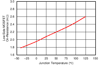
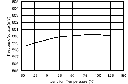
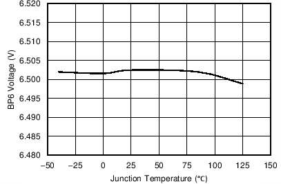
| IBP6 = 25 mA |
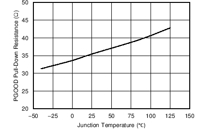
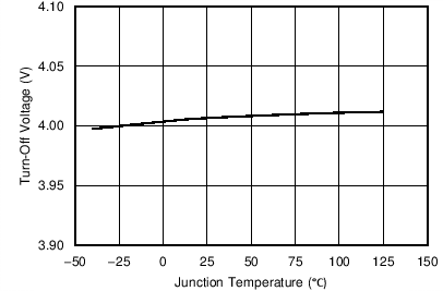
| VIN_OFF = 4.00 V |
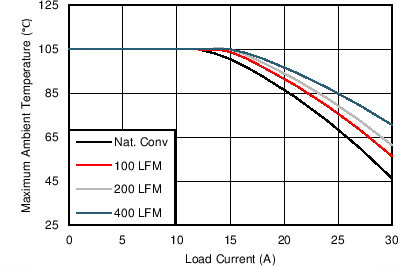
| VIN = 12 V | VOUT = 0.9 V | fSW = 300 kHz |
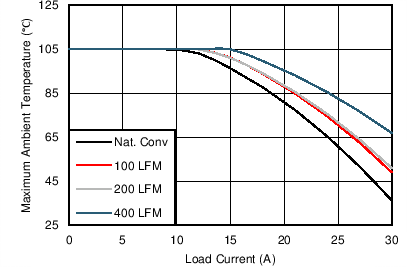
| VIN = 12 V | VOUT = 1.8 V | fSW = 300 kHz |
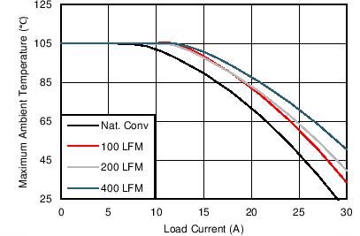
| VIN = 12 V | VOUT = 3.3 V | fSW = 300 kHz |
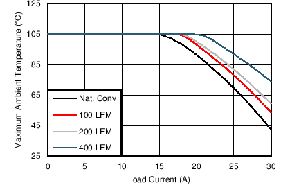
| VIN = 5 V | VOUT = 0.9 V | fSW = 300 kHz |
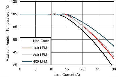
| VIN = 5 V | VOUT = 1.8 V | fSW = 300 kHz |
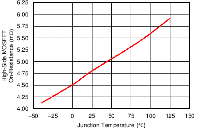
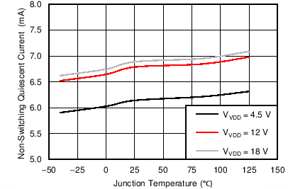
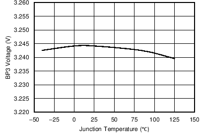
| IBP3 = 5 mA |
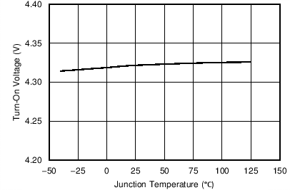
| VIN_ON = 4.25 V |
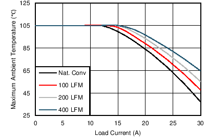
| VIN = 12 V | VOUT = 0.9 V | fSW = 650 kHz |
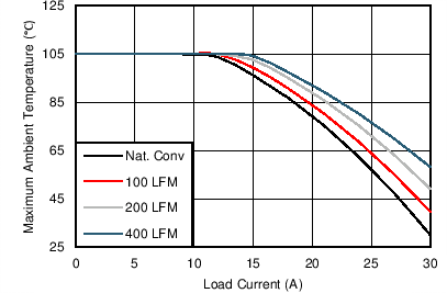
| VIN = 12 V | VOUT =1.8 V | fSW = 650 kHz |
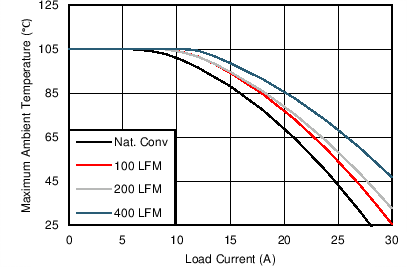
| VIN = 12 V | VOUT = 3.3 V | fSW = 650 kHz |
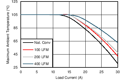
| VIN = 5 V | VOUT = 0.9 V | fSW = 650 kHz |
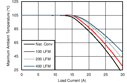
| VIN = 5 V | VOUT = 1.8 V | fSW = 650 kHz |