ZHCSDR7 May 2015 TPS54334
PRODUCTION DATA.
- 1 特性
- 2 应用
- 3 说明
- 4 简化电路原理图
- 5 修订历史记录
- 6 Pin Configuration and Functions
- 7 Specifications
-
8 Detailed Description
- 8.1 Overview
- 8.2 Functional Block Diagram
- 8.3
Feature Description
- 8.3.1 Fixed Frequency PWM Control
- 8.3.2 Light Load Operation
- 8.3.3 Slope Compensation and Output Current
- 8.3.4 Bootstrap Voltage (BOOT) and Low Dropout Operation
- 8.3.5 Error Amplifier
- 8.3.6 Voltage Reference
- 8.3.7 Adjusting the Output Voltage
- 8.3.8 Enable and Undervoltage Lockout
- 8.3.9 Slow Start
- 8.3.10 Safe Start-up into Pre-Biased Outputs
- 8.3.11 Power Good (PGOOD)
- 8.4 Device Functional Modes
-
9 Application and Implementation
- 9.1 Application Information
- 9.2
Typical Applications
- 9.2.1
TPS54334 Application
- 9.2.1.1 Design Requirements
- 9.2.1.2 Detailed Design Procedure
- 9.2.1.3 Application Curves
- 9.2.1
TPS54334 Application
- 10Power Supply Recommendations
- 11Layout
- 12器件和文档支持
- 13机械、封装和可订购信息
封装选项
机械数据 (封装 | 引脚)
散热焊盘机械数据 (封装 | 引脚)
订购信息
8 Detailed Description
8.1 Overview
The device is a 28-V, 3-A, synchronous step-down (buck) converter with two integrated n-channel MOSFETs. To improve performance during line and load transients the device implements a constant frequency, peak current mode control which reduces output capacitance and simplifies external frequency compensation design.
The device is designed for safe monotonic startup into pre-biased loads. It has a typical default start up voltage of 3.9 V. The EN pin has an internal pull-up current source that can provide a default condition when the EN pin is floating for the device to operate. The total operating current for the device is typically 310µA when not switching and under no load. When the device is disabled, the supply current is less than 5μA.
The integrated 128mΩ/84mΩ MOSFETs allow for high efficiency power supply designs with continuous output currents up to 3 amperes.
The device reduces the external component count by integrating the boot recharge diode. The bias voltage for the integrated high-side MOSFET is supplied by a capacitor between the BOOT and SW pins. The boot capacitor voltage is monitored by an UVLO circuit and turns off the high-side MOSFET when the voltage falls below a preset threshold. The output voltage can be stepped down to as low as the 0.8 V reference.
The device has a power good comparator (PGOOD) with hysteresis which monitors the output voltage through the VSENSE pin. The PGOOD pin is an open drain MOSFET which is pulled low when the VSENSE pin voltage is less than 84% or greater than 116% of the reference voltage Vref and asserts high when the VSENSE pin voltage is 90% to 110% of the Vref.
The device minimizes excessive output over-voltage transients by taking advantage of the over-voltage power good comparator. When the regulated output voltage is greater than 116% of the nominal voltage, the over-voltage comparator is activated, and the high-side MOSFET is turned off and masked from turning on until the output voltage is lower than 110%.
The TPS54334 operating frequency is fixed at 570 kHz and at 2 ms slow start time.
8.2 Functional Block Diagram
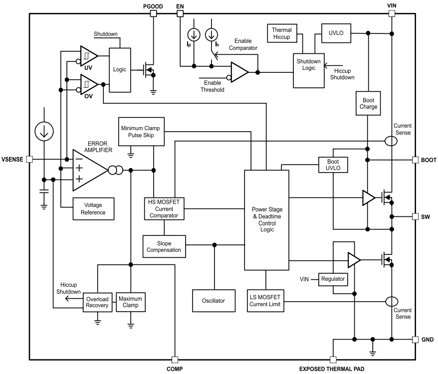
8.3 Feature Description
8.3.1 Fixed Frequency PWM Control
The device uses a fixed frequency, peak current mode control. The output voltage is compared through external resistors on the VSENSE pin to an internal voltage reference by an error amplifier which drives the COMP pin. An internal oscillator initiates the turn on of the high side power switch. The error amplifier output is compared to the high side power switch current. When the power switch current reaches the COMP voltage level the high side power switch is turned off and the low side power switch is turned on. The COMP pin voltage increases and decreases as the output current increases and decreases. The device implements a current limit by clamping the COMP pin voltage to a maximum level and also implements a minimum clamp for improved transient response performance.
8.3.2 Light Load Operation
The device monitors the peak switch current of the high-side MOSFET. Once the peak switch current is lower than typically 0.5A, the device stops switching to boost the efficiency until the peak switch current is again higher than typically 0.5A.
8.3.3 Slope Compensation and Output Current
The device adds a compensating ramp to the switch current signal. This slope compensation prevents sub-harmonic oscillations as duty cycle increases. The available peak inductor current remains constant over the full duty cycle range.
8.3.4 Bootstrap Voltage (BOOT) and Low Dropout Operation
The device has an integrated boot regulator and requires a small ceramic capacitor between the BOOT and SW pin to provide the gate drive voltage for the high-side MOSFET. The value of the ceramic capacitor should be 0.1μF. A ceramic capacitor with an X7R or X5R grade dielectric with a voltage rating of 10 V or higher is recommended because of the stable characteristics over temperature and voltage.
When the voltage between BOOT and SW pins drops below the BOOT-SW UVLO threshold, which is 2.2 V (typical), the high-side MOSFET turns off and the low-side MOSFET turns on, allowing the boot capacitor to recharge.
The device may work at 100% duty ratio as long as the BOOT-SW voltage is higher than the BOOT-SW UVLO threshold; but, do not operate the device at 100% duty ratio with no load.
8.3.5 Error Amplifier
The device has a transconductance amplifier. The error amplifier compares the VSENSE voltage to the lower of the internal slow start voltage or the internal 0.8 V voltage reference. The transconductance of the error amplifier is 1300μA/V typically. The frequency compensation components are placed between the COMP pin and ground.
8.3.6 Voltage Reference
The voltage reference system produces a precise ±1.5% voltage reference over temperature by scaling the output of a temperature stable bandgap circuit. The bandgap and scaling circuits produce 0.8 V at the non-inverting input of the error amplifier.
8.3.7 Adjusting the Output Voltage
The output voltage is set with a resistor divider from the output node to the VSENSE pin. It is recommended to use divider resistors with 1% tolerance or better. Start with a 10 kΩ for the R1 resistor and use the Equation 1 to calculate R2. To improve efficiency at light loads consider using larger value resistors. If the values are too high the regulator is more susceptible to noise and voltage errors from the VSENSE input current are noticeable.

8.3.8 Enable and Undervoltage Lockout
The EN pin provides electrical on/off control of the device. Once the EN pin voltage exceeds the threshold voltage, the device starts operation. If the EN pin voltage is pulled below the threshold voltage, the regulator stops switching and enters the low-quiescent (IQ) state.
The EN pin has an internal pull-up current source, allowing the user to float the EN pin for enabling the device. If an application requires controlling the EN pin, use open drain or open collector output logic to interface with the pin
The device implements internal UVLO circuitry on the VIN pin. The device is disabled when the VIN pin voltage falls below the internal VIN UVLO threshold. The internal VIN UVLO threshold has a hysteresis of 180mV.
If an application requires a higher UVLO threshold on the VIN pin, then the EN pin can be configured as shown in Figure 13. When using the external UVLO function it is recommended to set the hysteresis to be greater than 500mV.
The EN pin has a small pull-up current Ip which sets the default state of the pin to enable when no external components are connected. The pull-up current is also used to control the voltage hysteresis for the UVLO function since it increases by Ih once the EN pin crosses the enable threshold. The UVLO thresholds can be calculated using Equation 2, and Equation 3.
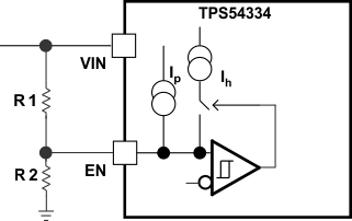 Figure 13. Adjustable VIN Undervoltage Lockout
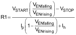
space

where
- IP = 1.15 μA
- IH = 3.3 μA
- VENfalling = 1.17 V
- VENrising = 1.21 V
8.3.9 Slow Start
The internal 2-ms soft-start time is implemented to minimize inrush currents. If during normal operation, the VIN goes below the UVLO, EN pin pulled below 1.21 V, or a thermal shutdown event occurs, the device stops switching and the internal slow start voltage is discharged to 0 volts before reinitiating a powering up sequence.
8.3.10 Safe Start-up into Pre-Biased Outputs
The device is designed to prevent the low-side MOSFET from discharging a pre-biased output. During monotonic pre-biased startup, both high-side and low-side MOSFETs are not allowed to be turned on until the internal soft-start voltage is higher than VSENSE pin voltage.
8.3.11 Power Good (PGOOD)
The PGOOD pin is an open drain output. Once the VSENSE pin is between 90% and 110% of the internal voltage reference the PGOOD pin pull-down is de-asserted and the pin floats. It is recommended to use a pull up resistor between the values of 10kΩ and 100kΩ to a voltage source that is 5.5V or less. The PGOOD is in a defined state once the VIN input voltage is greater than 1V but with reduced current sinking capability. The PGOOD achieves full current sinking capability once the VIN input voltage is above 4.2V.
The PGOOD pin is pulled low when VSENSE is lower than 84% or greater than 116% of the nominal internal reference voltage. Also, the PGOOD is pulled low, if the input UVLO or thermal shutdown is asserted, the EN pin is pulled low.
8.4 Device Functional Modes
8.4.1 Overcurrent/Overvoltage/Thermal Protection
The device is protected from output overvoltage, overload and thermal fault conditions. The device minimizes excessive output overvoltage transients by taking advantage of the overvoltage circuit power good comparator. When the overvoltage comparator is activated, the high-side MOSFET is turned off and prevented from turning on until the VSENSE pin voltage is lower than 106% of the Vref. The device implements both high-side MOSFET overload protection and bidirectional low-side MOSFET overload protections which help control the inductor current and avoid current runaway. If the overcurrent condition has lasted for more than the hiccup wait time, the device will shut down and re-start after the hiccup time. The device also shuts down if the junction temperature is higher than thermal shutdown trip point. When the junction temperature drops 10°C typically below the thermal shutdown trip point, the built-in thermal shutdown hiccup timer is triggered. The device will be restarted under control of the slow start circuit automatically after the thermal shutdown hiccup time is over.
Furthermore, if the overcurrent condition has lasted for more than the hiccup wait time which is programmed for 512 switching cycles, the device will shut down itself and re-start after the hiccup time which is set for 16384 cycles. The hiccup mode helps to reduce the device power dissipation under severe overcurrent conditions.
8.4.2 Thermal Shutdown
The internal thermal shutdown circuitry forces the device to stop switching if the junction temperature exceeds 165°C typically. Once the junction temperature drops below 155°C typically, the internal thermal hiccup timer will start to count. The device reinitiates the power up sequence after the built-in thermal shutdown hiccup time (32768 cycles) is over.
8.4.3 Small Signal Model for Loop Response
Figure 14 shows an equivalent model for the device control loop which can be modeled in a circuit simulation program to check frequency response and transient responses. The error amplifier is a trans conductance amplifier with a gm of 1300μA/V. The error amplifier can be modeled using an ideal voltage controlled current source. The resistor Roea (3.07 MΩ) and capacitor Coea (20.7 pF) model the open loop gain and frequency response of the error amplifier. The 1-mV ac voltage source between the nodes a and b effectively breaks the control loop for the frequency response measurements. Plotting a/c and c/b show the small signal responses of the power stage and frequency compensation respectively. Plotting a/b shows the small signal response of the overall loop. The dynamic loop response can be checked by replacing the RL with a current source with the appropriate load step amplitude and step rate in a time domain analysis.
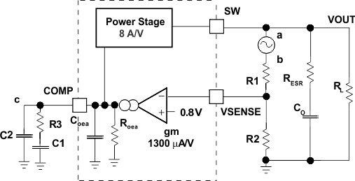 Figure 14. Small Signal Model for Loop Response
8.4.4 Small Signal Model for Peak Current Mode Control
Figure 15 is a simple small signal model that can be used to understand how to design the frequency compensation. The device power stage can be approximated to a voltage controlled current source (duty cycle modulator) supplying current to the output capacitor and load resistor. The control to output transfer function is shown in Equation 4 and consists of a dc gain, one dominant pole and one ESR zero. The quotient of the change in switch current and the change in COMP pin voltage (node c in Figure 14) is the power stage trans conductance (gmps) which is 8 A/V for the device. The DC gain of the power stage is the product of gmps and the load resistance, RL, as shown in Equation 6 with resistive loads. As the load current increases, the DC gain decreases. This variation with load may seem problematic at first glance, but fortunately the dominant pole moves with load current (see Equation 6). The combined effect is highlighted by the dashed line in Figure 16. As the load current decreases, the gain increases and the pole frequency lowers, keeping the 0-dB crossover frequency the same for the varying load conditions which makes it easier to design the frequency compensation.
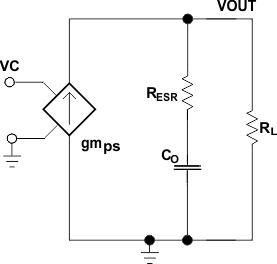 Figure 15. Small Signal Model for Peak Current Mode Control
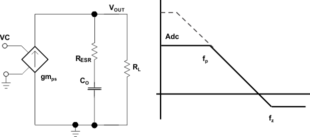 Figure 16. Simplified Frequency Response for Peak Current Mode Control
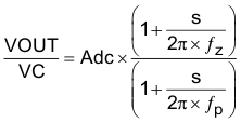


Where
gmea is the GM amplifier gain (1300µA/V)
gmPS is the power stage gain (8A/V)
RL is the load resistance
CO is the output capacitance
RESR is the equivalent series resistance of the output capacitors
8.4.5 Small Signal Model for Frequency Compensation
The device uses a transconductance amplifier for the error amplifier and readily supports two of the commonly used Type II compensation circuits and a Type III frequency compensation circuit, as shown in Figure 17. In Type 2A, one additional high frequency pole, C6, is added to attenuate high frequency noise. In Type III, one additional capacitor, C11, is added to provide a phase boost at the crossover frequency. See Designing Type III Compensation for Current Mode Step-Down Converters (SLVA352) for a complete explanation of Type III compensation.
The design guidelines below are provided for advanced users who prefer to compensate using the general method. The below equations only apply to designs whose ESR zero is above the bandwidth of the control loop. This is usually true with ceramic output capacitors.
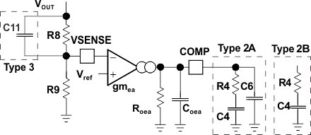 Figure 17. Types of Frequency Compensation
The general design guidelines for device loop compensation are as follows:
1. Determine the crossover frequency, fc. A good starting point is 1/10th of the switching frequency, fsw.
2. R4 can be determined by:

where
- gmea is the GM amplifier gain (1300µA/V)
- gmPS is the power stage gain (8A/V)
- Vref is the reference voltage (0.8V)
3. Place a compensation zero at the dominant pole:

4. C4 can be determined by:

5. C6 is optional. It can be used to cancel the zero from the ESR of the output capacitor Co

6. Type III compensation can be implemented with the addition of one capacitor, C11. This allows for slightly higher loop bandwidths and higher phase margins. If used, C11 can be estimated from Equation 12.
