ZHCSDR7 May 2015 TPS54334
PRODUCTION DATA.
- 1 特性
- 2 应用
- 3 说明
- 4 简化电路原理图
- 5 修订历史记录
- 6 Pin Configuration and Functions
- 7 Specifications
-
8 Detailed Description
- 8.1 Overview
- 8.2 Functional Block Diagram
- 8.3
Feature Description
- 8.3.1 Fixed Frequency PWM Control
- 8.3.2 Light Load Operation
- 8.3.3 Slope Compensation and Output Current
- 8.3.4 Bootstrap Voltage (BOOT) and Low Dropout Operation
- 8.3.5 Error Amplifier
- 8.3.6 Voltage Reference
- 8.3.7 Adjusting the Output Voltage
- 8.3.8 Enable and Undervoltage Lockout
- 8.3.9 Slow Start
- 8.3.10 Safe Start-up into Pre-Biased Outputs
- 8.3.11 Power Good (PGOOD)
- 8.4 Device Functional Modes
-
9 Application and Implementation
- 9.1 Application Information
- 9.2
Typical Applications
- 9.2.1
TPS54334 Application
- 9.2.1.1 Design Requirements
- 9.2.1.2 Detailed Design Procedure
- 9.2.1.3 Application Curves
- 9.2.1
TPS54334 Application
- 10Power Supply Recommendations
- 11Layout
- 12器件和文档支持
- 13机械、封装和可订购信息
封装选项
机械数据 (封装 | 引脚)
散热焊盘机械数据 (封装 | 引脚)
订购信息
7 Specifications
7.1 Absolute Maximum Ratings
over operating free-air temperature range (unless otherwise noted) (1)(2)| MIN | MAX | UNIT | ||
|---|---|---|---|---|
| Input Voltage | VIN | –0.3 | 30 | V |
| EN | –0.3 | 6 | V | |
| BOOT | –0.3 | (SW+7.5) | V | |
| VSENSE | –0.3 | 3 | V | |
| COMP | –0.3 | 3 | V | |
| PGOOD | –0.3 | 6 | V | |
| Output Voltage | BOOT-SW | 0 | 7.5 | V |
| SW | –1 | 30 | V | |
| SW 10ns Transient | –3.5 | 30 | V | |
| Vdiff(GND to Exposed Thermal Pad) | –0.2 | 0.2 | V | |
| Source Current | EN | 100 | µA | |
| SW | Current Limit | A | ||
| Sink Current | SW | Current Limit | A | |
| COMP | 200 | 200 | µA | |
| PGOOD | –0.1 | 5 | mA | |
| Operating Junction Temperature | –40 | 150 | °C | |
| Storage temperature, Tstg | –65 | 150 | ||
(1) Stresses beyond those listed under Absolute Maximum Ratings may cause permanent damage to the device. These are stress ratings only, which do not imply functional operation of the device at these or any other conditions beyond those indicated under Recommended Operating Conditions. Exposure to absolute-maximum-rated conditions for extended periods may affect device reliability.
(2) The human body model is a 100-pF capacitor discharged through a 1.5-kΩ resistor into each pin. The machine model is a 200-pF capacitor discharged directly into each pin.
7.2 ESD Ratings
| VALUE | UNIT | ||||
|---|---|---|---|---|---|
| V(ESD) | Electrostatic discharge | Human body model (HBM), per ANSI/ESDA/JEDEC JS-001, all pins(1) | ±2000 | V | |
| Charged device model (CDM), per JEDEC specification JESD22-C101, all pins(2) | ±500 | V | |||
(1) JEDEC document JEP155 states that 500-V HBM allows safe manufacturing with a standard ESD control process.
(2) JEDEC document JEP157 states that 250-V CDM allows safe manufacturing with a standard ESD control process.
7.3 Recommended Operating Conditions
over operating free-air temperature range (unless otherwise noted)| MIN | MAX | UNIT | |||
|---|---|---|---|---|---|
| VSS | Supply input voltage | 4.2 | 28 | V | |
| VOUT | Output voltage | 0.8 | 24 | V | |
| IOUT | Output current | 0 | 3 | A | |
| TJ | Operating junction temperature(1) | –40 | 150 | °C | |
(1) The device must operate within 150°C to ensure continuous function and operation of the device.
7.4 Thermal Information
| THERMAL METRIC(1) | TPS54334 | UNIT | ||
|---|---|---|---|---|
| DDA (8 PINS) | DRC (10 Pins) | |||
| RθJA | Junction-to-ambient thermal resistance | 42.1 | 43.9 | °C/W |
| RθJC(top) | Junction-to-case (top) thermal resistance | 50.9 | 55.4 | °C/W |
| RθJB | Junction-to-board thermal resistance | 31.8 | 18.9 | °C/W |
| ψJT | Junction-to-top characterization parameter | 5 | 0.7 | °C/W |
| ψJB | Junction-to-board characterization parameter | 13.5 | 19.1 | °C/W |
| RθJC(bot) | Junction-to-case (bottom) thermal resistance | 7.1 | 5.3 | °C/W |
(1) For more information about traditional and new thermal metrics, see the IC Package Thermal Metrics application report, SPRA953.
7.5 Electrical Characteristics
The Electrical Ratings specified in this section will apply to all specifications in this document unless otherwise noted. These specifications will be interpreted as conditions that will not degrade the device’s parametric or functional specifications for the life of the product containing it. TJ = –40°C to 150°C, VIN =4.2 to 28V, (unless otherwise noted)| PARAMETER | TEST CONDITIONS | MIN | TYP | MAX | UNIT |
|---|---|---|---|---|---|
| SUPPLY VOLTAGE AND UVLO (VIN PIN) | |||||
| Operating input voltage | 4.2 | 28 | V | ||
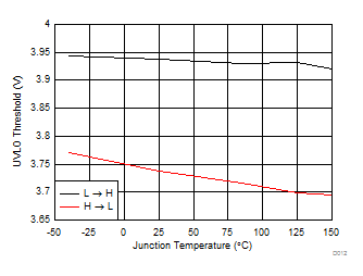
| Input UVLO threshold | Rising Vin | 3.9 | 4.2 | V | |
| Input UVLO hysteresis | 180 | 400 | mV | ||
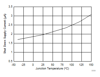
| VIN Shutdown Supply Current | EN = 0V | 2 | 10 | µA | |
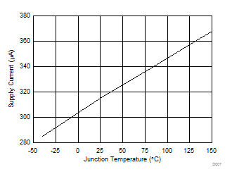
| VIN Operating– non switching supply current | VSENSE=810mV | 310 | 800 | µA | |
| ENABLE (EN PIN) | |||||
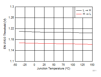
| Enable threshold | Rising | 1.21 | 1.28 | V | |
| Enable threshold | Falling | 1.1 | 1.17 | V | |
| Input current | EN=1.1V | 1.15 | µA | ||
| Hysteresis current | EN=1.3V | 3.3 | µA | ||
| VOLTAGE REFERENCE | |||||
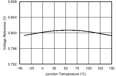
| Reference | TJ = 25°C | 0.792 | 0.8 | 0.808 | V |
| 0.788 | 0.8 | 0.812 | V | ||
| MOSFET | |||||
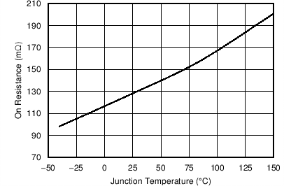
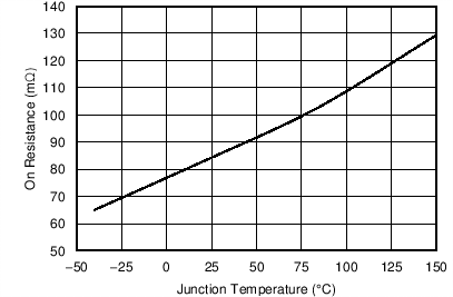
| High side switch resistance(1) | BOOT-SW = 3V | 160 | 290 | mΩ | |
| BOOT-SW = 6V | 128 | 240 | mΩ | ||
| Low side switch resistance(1) | 84 | 170 | mΩ | ||
| ERROR AMPLIFIER | |||||
| Error amplifier transconductance (gm) | –2 µA < ICOMP < 2 µA V(COMP)=1V | 1300 | µmhos | ||
| Error amplifier source/sink | V(COMP)=1V, 100 mV Overdrive | 100 | µA | ||
| Start switching peak current threshold | 0.5 | A | |||
| COMP to Iswitch gm | 8 | A/V | |||
| CURRENT LIMIT | |||||
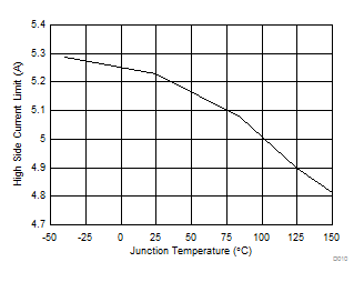
| High side switch current limit threshold | 4 | 5.2 | 6.5 | A | |
| Low side switch sourcing current limit | 3.5 | 4.7 | 6.1 | A | |
| Low side switch sinking current limit | 0 | A | |||
| Hiccup wait time | 512 | Cycles | |||
| Hiccup time before re-start | 16384 | Cycles | |||
| THERMAL SHUTDOWN | |||||
| Thermal shutdown | 165 | °C | |||
| Thermal shutdown hysterisis | 10 | °C | |||
| Thermal shutdown hiccup time | 32768 | Cycles | |||
| SW (SW PIN) | |||||
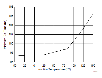
| Minimum on time | Measured at 90% to 90% of VIN, ISW = 2A | 94 | 145 | ns | |
| Minimum off time | BOOT-SW ≥ 3V | 0% | |||
| BOOT (BOOT PIN) | |||||
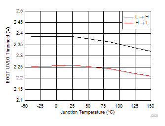
| BOOT-SW UVLO | 2.2 | 3 | V | ||
| SLOW START | |||||
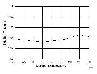
| Internal slow start time | 2 | ms | |||
| SWITCHING FREQUENCY | |||||
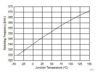
| Internal switching frequency | 456 | 570 | 684 | kHz | |
| POWER GOOD (PGOOD PIN) | |||||
| VSENSE falling (Fault) | 84 | % Vref | |||
| VSENSE rising (Good) | 90 | % Vref | |||
| VSENSE rising (Fault) | 116 | % Vref | |||
| VSENSE falling (Good) | 110 | % Vref | |||
| Output high leakage | VSENSE = Vref, V(PGOOD) = 5.5 V | 30 | 500 | nA | |
| Output low | I(PGOOD) = 0.35 mA | 0.3 | V | ||
| Minimum VIN for valid output(2) | V(PGOOD) < 0.5V at 100 µA | 0.6 | 1 | V | |
| MAXIMUM OUTPUT VOLTAGE UNDER MINIMUM VIN(2) | |||||
| Maximum output voltage | VIN = 4.2V, Iout = 3A | 2.9 | V | ||
| VIN = 4.2V, Iout = 2.5A | 3.2 | ||||
| VIN = 4.2V, Iout = 2A | 3.4 | ||||
| VIN = 4.2V, Iout = 1.5A | 3.5 | ||||
(1) Measured at pins.
(2) Not tested for mass production.
7.6 Typical Characteristics
VIN = 12 V, unless otherwise specified.