ZHCSQS0E August   2006  – January 2024 TPS5410

PRODUCTION DATA  

  1.   1
  2. 特性
  3. 应用
  4. 说明
  5. Pin Configuration and Functions
  6. Specifications
    1. 5.1 Absolute Maximum Ratings
    2. 5.2 ESD Ratings
    3. 5.3 Recommended Operating Conditions
    4. 5.4 Thermal Information 
    5. 5.5 Electrical Characteristics
    6. 5.6 Typical Characteristics
  7. Detailed Description
    1. 6.1 Overview
    2. 6.2 Functional Block Diagram
    3. 6.3 Feature Description
      1. 6.3.1  Oscillator Frequency
      2. 6.3.2  Voltage Reference
      3. 6.3.3  Enable (ENA) and Internal Slow-Start
      4. 6.3.4  Undervoltage Lockout (UVLO)
      5. 6.3.5  Boost Capacitor (BOOT)
      6. 6.3.6  Output Feedback (VSENSE)
      7. 6.3.7  Internal Compensation
      8. 6.3.8  Voltage Feed-Forward
      9. 6.3.9  Pulse-Width-Modulation (PWM) Control
      10. 6.3.10 Overcurrent Limiting
      11. 6.3.11 Overvoltage Protection
      12. 6.3.12 Thermal Shutdown
    4. 6.4 Device Functional Modes
      1. 6.4.1 Minimum Input Voltage
      2. 6.4.2 ENA Control
  8. Applications and Implementation
    1. 7.1 Application Information
    2. 7.2 Typical Applications
      1. 7.2.1 Application Circuit
        1. 7.2.1.1 Design Requirements
        2. 7.2.1.2 Detailed Design Procedure
          1. 7.2.1.2.1 Switching Frequency
          2. 7.2.1.2.2 Input Capacitors
          3. 7.2.1.2.3 Output Filter Components
            1. 7.2.1.2.3.1 Inductor Selection
            2. 7.2.1.2.3.2 Capacitor Selection
          4. 7.2.1.2.4 Output Voltage Setpoint
          5. 7.2.1.2.5 Boot Capacitor
          6. 7.2.1.2.6 Catch Diode
          7. 7.2.1.2.7 Advanced Information
            1. 7.2.1.2.7.1 Output Voltage Limitations
            2. 7.2.1.2.7.2 Internal Compensation Network
            3. 7.2.1.2.7.3 Thermal Calculations
        3. 7.2.1.3 Application Curves
      2. 7.2.2 Using All Ceramic Capacitors
        1. 7.2.2.1 Design Requirements
        2. 7.2.2.2 Detailed Design Procedure
          1. 7.2.2.2.1 Output Filter Capacitor Selection
          2. 7.2.2.2.2 External Compensation Network
        3. 7.2.2.3 Application Curves
    3. 7.3 Power Supply Recommendations
    4. 7.4 Layout
      1. 7.4.1 Layout Guidelines
      2. 7.4.2 Layout Example
  9. Device and Documentation Support
    1. 8.1 Documentation Support
      1. 8.1.1 Related Documentation
    2. 8.2 接收文档更新通知
    3. 8.3 支持资源
    4. 8.4 Trademarks
    5. 8.5 静电放电警告
    6. 8.6 术语表
  10. Revision History
  11. 10Mechanical, Packaging, and Orderable Information

封装选项

机械数据 (封装 | 引脚)
散热焊盘机械数据 (封装 | 引脚)
订购信息

说明

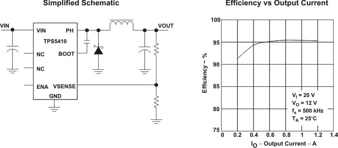
TPS5410 是一款高输出电流 PWM 转换器,集成了低电阻高侧 N 沟道 MOSFET。具有所列特性的基板上还包括高性能电压误差放大器(可在瞬态条件下提供高稳压精度)、欠压锁定电路(用于防止在输入电压达到 5.5V 前启动)、内部设置的慢启动电路(用于限制浪涌电流)以及电压前馈电路(用于改进瞬态响应)。通过使用 ENA 引脚,关断电源电流通常可减少到 18μA。其他特性包括高电平有效使能端、过流限制、过压保护和热关断。为降低设计复杂性并减少外部元件数量,TPS5410 反馈环路进行了内部补偿。

TPS5410 器件采用易于使用的 8 引脚 SOIC 封装。TI 提供评估模块和软件工具,有助于快速实现高性能电源设计,可满足迫切的设备开发周期要求。

封装信息
器件型号封装(1)封装尺寸(2)
TPS5410D(SOIC,8)4.9mm × 6mm
有关更多信息,请参阅 节 10
封装尺寸(长 × 宽)为标称值,并包括引脚(如适用)。
GUID-4FABC4C3-0639-4314-A987-BB763970B015-low.gif