ZHCSQS0E August 2006 – January 2024 TPS5410
PRODUCTION DATA
- 1
- 1 特性
- 2 应用
- 3 说明
- 4 Pin Configuration and Functions
- 5 Specifications
-
6 Detailed Description
- 6.1 Overview
- 6.2 Functional Block Diagram
- 6.3
Feature Description
- 6.3.1 Oscillator Frequency
- 6.3.2 Voltage Reference
- 6.3.3 Enable (ENA) and Internal Slow-Start
- 6.3.4 Undervoltage Lockout (UVLO)
- 6.3.5 Boost Capacitor (BOOT)
- 6.3.6 Output Feedback (VSENSE)
- 6.3.7 Internal Compensation
- 6.3.8 Voltage Feed-Forward
- 6.3.9 Pulse-Width-Modulation (PWM) Control
- 6.3.10 Overcurrent Limiting
- 6.3.11 Overvoltage Protection
- 6.3.12 Thermal Shutdown
- 6.4 Device Functional Modes
-
7 Applications and Implementation
- 7.1 Application Information
- 7.2
Typical Applications
- 7.2.1 Application Circuit
- 7.2.2 Using All Ceramic Capacitors
- 7.3 Power Supply Recommendations
- 7.4 Layout
- 8 Device and Documentation Support
- 9 Revision History
- 10Mechanical, Packaging, and Orderable Information
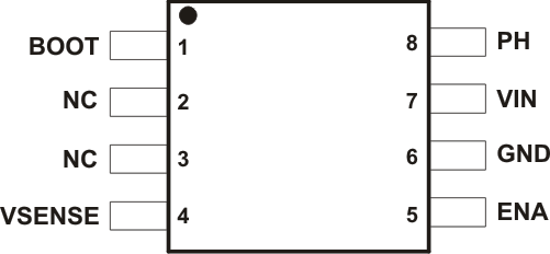
4 Pin Configuration and Functions
 Figure 4-1 D
Package,8 Pin SOICTop View
Figure 4-1 D
Package,8 Pin SOICTop ViewTable 4-1 Pin Functions
| PIN | I/O | DESCRIPTION | |
|---|---|---|---|
| NAME | NO. | ||
| BOOT | 1 | O | Boost capacitor for the high-side FET gate driver. Connect 0.01 μF low ESR capacitor from BOOT pin to PH pin. |
| NC | 2, 3 | — | Not connected internally. |
| VSENSE | 4 | I | Feedback voltage for the regulator. Connect to output voltage divider. |
| ENA | 5 | I | On and off control. Below 0.5 V, the device stops switching. Float the pin to enable. |
| GND | 6 | — | Ground. |
| VIN | 7 | I | Input supply voltage. Bypass VIN pin to GND pin close to device package with a high quality, low ESR ceramic capacitor. |
| PH | 8 | O | Source of the high side power MOSFET. Connected to external inductor and diode. |