ZHCSED1A November   2015  – November 2015 TPS53317A

PRODUCTION DATA.  

  1. 特性
  2. 应用
  3. 说明
  4. 修订历史记录
  5. Pin Configuration and Functions
  6. Specifications
    1. 6.1 Absolute Maximum Ratings
    2. 6.2 ESD Ratings
    3. 6.3 Recommended Operating Conditions
    4. 6.4 Thermal Information
    5. 6.5 Electrical Characteristics
    6. 6.6 Typical Characteristics
  7. Detailed Description
    1. 7.1 Overview
    2. 7.2 Functional Block Diagram
    3. 7.3 Feature Description
      1. 7.3.1 PWM Operation
      2. 7.3.2 PWM Frequency and Adaptive On-Time Control
      3. 7.3.3 Light-Load Power Saving Features
      4. 7.3.4 Power Sequences
        1. 7.3.4.1 Non-Tracking Startup
        2. 7.3.4.2 Tracking Startup
      5. 7.3.5 Protection Features
        1. 7.3.5.1 5-V Undervoltage Protection (UVLO)
        2. 7.3.5.2 Power Good Signals
        3. 7.3.5.3 Output Overvoltage Protection (OVP)
        4. 7.3.5.4 Output Undervoltage Protection (UVP)
        5. 7.3.5.5 Overcurrent Protection
          1. 7.3.5.5.1 Overcurrent Limit
          2. 7.3.5.5.2 Negative OCL
      6. 7.3.6 Thermal Protection
    4. 7.4 Device Functional Modes
      1. 7.4.1 Non-Droop Configuration
      2. 7.4.2 Droop Configuration
  8. Application and Implementation
    1. 8.1 Application Information
    2. 8.2 Typical Applications
      1. 8.2.1 DDR4 SDRAM Application
        1. 8.2.1.1 Design Requirements
        2. 8.2.1.2 Detailed Design Procedure
          1. 8.2.1.2.1 Step 1. Determine Configuration
          2. 8.2.1.2.2 Step 2. Select Inductor
          3. 8.2.1.2.3 Step 3. Determine Output Capacitance
          4. 8.2.1.2.4 Step 4. Input Capacitance
          5. 8.2.1.2.5 Step 5. Compensation Network
          6. 8.2.1.2.6 Peripheral Component Selection
        3. 8.2.1.3 Application Curves
      2. 8.2.2 DDR3 SDRAM Application
        1. 8.2.2.1 Design Requirements
      3. 8.2.3 Non-Tracking Point-of-Load (POL) Application
        1. 8.2.3.1 Design Requirements
        2. 8.2.3.2 Application Curves
  9. Power Supply Recommendations
  10. 10Layout
    1. 10.1 Layout Guidelines
    2. 10.2 Layout Example
  11. 11器件和文档支持
    1. 11.1 社区资源
    2. 11.2 商标
    3. 11.3 静电放电警告
    4. 11.4 Glossary
  12. 12机械、封装和可订购信息

封装选项

机械数据 (封装 | 引脚)
散热焊盘机械数据 (封装 | 引脚)
订购信息

10 Layout

10.1 Layout Guidelines

Stable power supply operation depends on proper layout. Follow these guidelines for an optimized PCB layout.

  • Connect PGND pins to the thermal pad underneath the device. Use four vias to connect the thermal pad to internal ground planes.
  • Place VIN, V5IN and VREF decoupling capacitors as close to the device as possible.
  • Use wide traces for the VIN, PGND and SW pins. These nodes carry high current and also serve as heat sinks.
  • Place feedback and compensation components as close to the device as possible.
  • Place COMP and VOUT analog signal traces away from noisy signals (SW, BST).
  • The GND pin should connect to the PGND in only one place, through a via or a 0-Ω resistor.

10.2 Layout Example
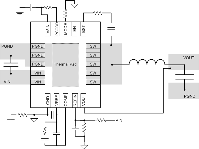
TPS53317A layout_slusak4.gif Figure 42. TPS53317A Board Layout