SLUSDW9A June 2020 – June 2020 TPS51215A
PRODUCTION DATA.
- 1 Features
- 2 Applications
- 3 Description
- 4 Revision History
- 5 Pin Configuration and Functions
- 6 Specifications
-
7 Detailed Description
- 7.1 Overview
- 7.2 Functional Block Diagram
- 7.3
Feature Description
- 7.3.1 Switch Mode Power Supply Control
- 7.3.2 VREF, V0, V1, V2, V3 and Output Voltage
- 7.3.3 Soft-Start and Power Good
- 7.3.4 SLEW and VID Function
- 7.3.5 MODE Pin Configuration
- 7.3.6 Light-Load Operation
- 7.3.7 Out-of-Bound Operation
- 7.3.8 Current Sensing and Overcurrent Protection
- 7.3.9 Overvoltage and Undervoltage Protection
- 7.3.10 V5IN Undervoltage Lockout Protection
- 7.3.11 Thermal Shutdown
- 7.4 D-CAP2 Control Mode
- 8 Application and Implementation
-
9 Typical Applications
- 9.1 Design Requirements
- 9.2
Detailed Design Procedure
- 9.2.1 Step One: Determine the Specifications
- 9.2.2 Step Two: Determine System Parameters
- 9.2.3 Step Three: Determine Inductor Value and Choose Inductor
- 9.2.4 Step Four: Set the Output Voltages
- 9.2.5 Step Five: Calculate SLEW Capacitance
- 9.2.6 Step Six
- 9.2.7 Step Seven: Determine the Output Capacitance
- 9.2.8 Step Eight: Select Decoupling and Peripheral Components
- 9.3 Application Examples
- 9.4 Application Curves of Design 1
- 10Power Supply Recommendations
- 11Layout
- 12Device and Documentation Support
- 13Mechanical, Packaging, and Orderable Information
7.3.4 SLEW and VID Function
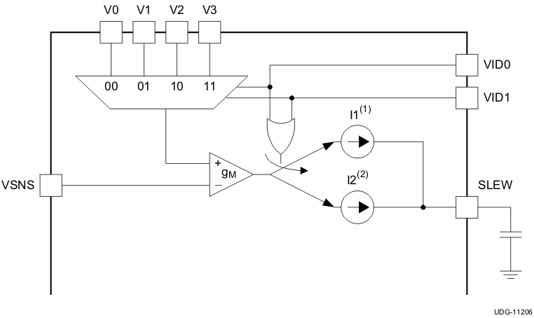
In addition to providing soft start function, SLEW is also used to program the VID transition time. TPS51215A supports 2-bit VID and 1-bit VID operations. VID0 and VID1 works with 1.05-V logic level signals with capability of supporting up to 3.3-V logic high.

(1) I1: Enable during VID transitioning, 45 µA.
(2) I2: Soft start, 4.5 µA.
Figure 8. VID Configuration During VID transition:
- SLEW current is increased to 45 µA. Based on the VID transition time of the system, the amount of the SLEW capacitance can be calculated to meet such requirement. The minimum SLEW capacitance can be supported by the device is 2nF.
- ISLEW is 45 µA, dV is the voltage change during VID transition
- dt is the required transition time
- FCCM (forced continuous conduction mode) operation is used regardless of the load level. In the meantime, the overcurrent level is temporality increased to 125% times the normal OCL level to prevent false OC trip during fast SLEW up transition. Power good, UVP and OVP functions are all blanked as well. All normal functions are resumed 16 internal clock cycles (64 µs) after VID transition is completed.
- Additional SLEW CLAMP is implemented. If severe output short occurs (either to GND or to some other high voltage rails in the system), SLEW is engaged into SLEW CLAMP, approximately 50 mV above or below the output voltage reference point. After 32 internal clockcycles, the CLAMP is engaged, UVP and OVP functions are activated to disable the controller at fault.
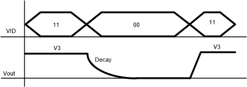
- If VID 00 is selected, part will enter low power mode where the DRVL and DRVH will be stop switching and Vout will decay to 0V. At mean time, the PGOOD pin still keeps high. The Vout transition time can be calculated by Equation 2
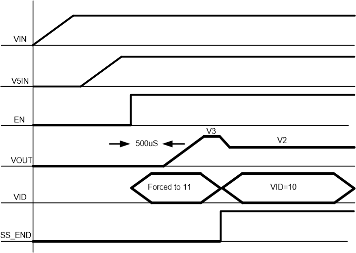
- VID is fixed to 11 internally until soft-start end which means that Vout ramp to V3 in soft start period. Figure 10 showed the power up sequence
Equation 2. 

where
 Figure 9. Low Power Mode Enter and Exit
  Figure 10. Power up Sequence