SLVS616C November 2005 – December 2014 TPS51124
PRODUCTION DATA.
- 1 Features
- 2 Applications
- 3 Description
- 4 Revision History
- 5 Pin Configuration and Functions
- 6 Specifications
- 7 Detailed Description
- 8 Application and Implementation
- 9 Power Supply Recommendations
- 10Layout
- 11Device and Documentation Support
- 12Mechanical, Packaging, and Orderable Information
封装选项
机械数据 (封装 | 引脚)
- RGE|24
散热焊盘机械数据 (封装 | 引脚)
- RGE|24
订购信息
6 Specifications
6.1 Absolute Maximum Ratings(1)
over operating free-air temperature range (unless otherwise noted)| MIN | MAX | UNIT | |||
|---|---|---|---|---|---|
| Input voltage | VBST1, VBST2 | –0.3 | 36 | V | |
| VBST1, VBST2 (wrt LLx) | –0.3 | 6 | |||
| V5IN, V5FILT, EN1, EN2, VFB1, VFB2, TRIP1, TRIP2, VO1, VO2, TONSEL | –0.3 | 6 | |||
| Output voltage | DRVH1, DRVH2 | –1 | 36 | V | |
| DRVH1, DRVH2 (wrt LLx) | –0.3 | 6 | |||
| LL1, LL2 | –2 | 30 | |||
| PGOOD1, PGOOD2, DRVL1, DRVL2 | –0.3 | 6 | |||
| PGND1, PGND2 | –0.3 | 0.3 | |||
| TA | Operating ambient temperature | –40 | 85 | °C | |
| TJ | Junction temperature | –40 | 125 | °C | |
| Tstg | Storage temperature | –55 | 150 | °C | |
(1) Stresses beyond those listed under absolute maximum ratings may cause permanent damage to the device. These are stress ratings only and functional operation of the device at these or any other conditions beyond those indicated under recommended operating conditions is not implied. Exposure to absolute-maximum-rated conditions for extended periods may affect device reliability. All voltage values are with respect to the network ground terminal unless otherwise noted
6.2 Recommended Operating Conditions
over operating free-air temperature (unless otherwise noted)| MIN | MAX | UNIT | |||
|---|---|---|---|---|---|
| Supply input voltage | V5IN, V5FILT | 4.5 | 5.5 | V | |
| Input voltage | VBST1, VBST2 | –0.1 | 34 | V | |
| VBST1, VBST2 (wrt LLx) | –0.1 | 5.5 | |||
| EN1, EN2, VFB1, VFB2, TRIP1, TRIP2, VO1, VO2, TONSEL | –0.1 | 5.5 | |||
| Output voltage | DRVH1, DRVH2 | –0.8 | 34 | V | |
| DRVH1, DRVH2 (wrt LLx) | –0.1 | 5.5 | |||
| LL1, LL2 | –1.8 | 28 | |||
| PGOOD1, PGOOD2, DRVL1, DRVL2 | –0.1 | 5.5 | |||
| PGND1, PGND2 | –0.1 | 0.1 | |||
| TA | Operating ambient temperature | –40 | 85 | °C | |
6.3 Thermal Information
| THERMAL METRIC(1) | TPS51124 | UNIT | |
|---|---|---|---|
| VQFN | |||
| 24 PINS | |||
| RθJA | Junction-to-ambient thermal resistance | 42.9 | °C/W |
(1) For more information about traditional and new thermal metrics, see the IC Package Thermal Metrics application report, SPRA953.
6.4 Electrical Characteristics
over operating free-air temperature range, V5IN = V5FILT = 5 V (unless otherwise noted)| PARAMETER | TEST CONDITIONS | MIN | TYP | MAX | UNIT | ||
|---|---|---|---|---|---|---|---|
| SUPPLY CURRENT | |||||||
| IV5FILT | V5FILT supply current | V5FILT current, no load, EN1 = EN2 = 5 V, VFB1 = VFB2 = 0.77 V, LL1=LL2=0.5V |
350 | 700 | μA | ||
| IV5INSDN | V5IN shutdown current | V5IN current, no load, EN1 = EN2 = 0 V | 1 | μA | |||
| IV5FILTSDN | V5FILT shutdown current | V5FILT current, no load, EN1 = EN2 = 0 V | 1 | μA | |||
| VFB VOLTAGE and DISCHARGE RESISTANCE | |||||||
| VVFB | VFB regulation voltage | FB voltage, skip mode (fPWM/10) | 764 | mV | |||
| VVFB | VFB regulation voltage tolerance | TA = 25°C, bandgap initial accuracy | –0.9% | 0.9% | |||
| TA = 0°C to 85°C(1) | –1.3% | 1.3% | |||||
| TA = –40°C to 85°C(1) | –1.6% | 1.6% | |||||
| VVFBSKIP | VFB regulation shift in continuous conduction | 0.758-V target for resistor divider. See PWM Operation of Detailed Description(1) | 758 | mV | |||
| IVFB | VFB input current | VFBx = 0.758 V, absolute value | 0.02 | 0.1 | μA | ||
| RDischg | VO discharge resistance | ENx = 0 V, VOx = 0.5 V, TA = 25°C | 10 | 20 | Ω | ||
| OUTPUT: N-CHANEEL MOSFET GATE DRIVERS | |||||||
| RDRVH | DRVH resistance | Source, VVBSTx–DRVHx = 0.5 V | 5 | 7 | Ω | ||
| Sink, VDRVHx-LLx= 0.5 V | 1.5 | 2.5 | Ω | ||||
| RDRVL | DRVL resistance | Source, VV5IN–DRVLx = 0.5 V | 4 | 6 | Ω | ||
| Sink, VDRVLx–PGNDx = 0.5 V | 1 | 2.0 | Ω | ||||
| TD | Dead time | DRVHx-low (DRVHx = 1 V) to DRVLx-on (DRVLx = 4 V), LL = –0.05 V, |
10 | 20 | 50 | ns | |
| DRVLx-low (DRVLx = 1 V) to DRVHx-on (DRVHx = 4 V), LL = –0.05 V, |
30 | 40 | 60 | ns | |||
| INTERNAL BST DIODE | |||||||
| VFBST | Forward voltage | VV5IN–VBSTx, IF = 10 mA, TA = 25°C | 0.7 | 0.8 | 0.9 | V | |
| IVBSTLK | VBST leakage current | VBST = 34 V, LL = 28 V, VOx = 5.5 V, TA = 25°C |
0.1 | 1 | μA | ||
| ON-TIME TIMER CONTROL AND INTERNAL SOFT START, | |||||||
| TON11 | CH1, 240-kHz setting | VO1 = 1.5 V,TONSEL = GND, LL1 = 12 V | 440 | 500 | 560 | ns | |
| TON12 | CH1, 300-kHz setting | VO1 = 1.5 V, TONSEL = FLOAT, LL1 = 12 V | 340 | 390 | 440 | ns | |
| TON13 | CH1, 360-kHz setting | VO1 = 1.5 V,TONSEL = V5FILT, LL1 = 12 V | 265 | 305 | 345 | ns | |
| TON21 | CH2, 300-kHz setting | VO2 = 1.05 V, TONSEL = GND, LL2 = 12 V | 235 | 270 | 305 | ns | |
| TON22 | CH2, 360-kHz setting | VO2 = 1.05 V, TONSEL = FLOAT, LL2 = 12 V | 180 | 210 | 240 | ns | |
| TON23 | CH2, 420-kHz setting | VO2 = 1.05 V, TONSEL = V5FILT, LL2 = 12 V | 120 | 150 | 180 | ns | |
| TON(MIN) | CH2 On time | VO2 = 0.76 V, TONSEL = V5FILT, LL2 = 28 V | 80 | 110 | 140 | ns | |
| TOFF(MIN) | CH1/CH2 Min. off time | LL = –0.1 V, TA= 25°C, VFB = 0.7 V | 435 | ns | |||
| Tss | Internal SS time | Internal soft start, time from ENx > 3 V to VFBx regulation value = 735 mV | 0.85 | 1.2 | 1.40 | ms | |
| UVLO/LOGIC THRESHOLD | |||||||
| VUV5VFILT | V5FILT UVLO threshold | Wake up | 3.7 | 4.0 | 4.3 | V | |
| Hysteresis | 0.2 | 0.3 | 0.4 | ||||
| VEN | ENx threshold | Wake up | 1.0 | 1.3 | 1.5 | V | |
| Hysteresis | 0.2 | ||||||
| IEN | ENx input current | Absolute value(2) | 0.02 | 0.1 | μA | ||
| VTONSEL | TONSEL threshold | Fast(2) | V5FILT –0.3 | V | |||
| Medium(2) | 2 | V5FILT –1.0 | |||||
| Slow(2) | 0.5 | ||||||
| ITONSEL | TONSEL input current | TONSEL=0V, current out of the pin(2) | 1 | μA | |||
| TONSEL=5V, current in to the pin(2) | 1 | ||||||
| CURRENT SENSE | |||||||
| ITRIP | TRIP source current | VTRIPx < 0.3 V, TA = 25°C | 9 | 10 | 11 | μA | |
| TCITRIP | ITRIP temperature coeffficent | On the basis of 25°C(2) | 4200 | ppm/°C | |||
| VOCLoff | OCP compensation offset | (VTRIPx-GND – VPGNDx-LLx) voltage, VTRIPx-GND = 60 mV |
–10 | 0 | 10 | mV | |
| VZC | Zero cross detection comparator offset | VPGNDx-LLx voltage, PGOODx = Hi(2) | 0.5 | mV | |||
| VRtrip | Current limit threshold setting range | VTRIPx-GND voltage, all temperatures(2) | 30 | 200 | mV | ||
| POWERGOOD COMPARATOR | |||||||
| VTHPG | PG threshold | PG in from lower (PGOODx goes hi) | 92.5% | 95% | 97.5% | ||
| PG low hysteresis (PGOODx goes low) | –5% | ||||||
| PG in from higher (PGOODx goes hi) | 102.5% | 105% | 107.5% | ||||
| PG high hysteresis (PGOODx goes low) | 5% | ||||||
| IPGMAX | PG sink current | PGOODx = 0.5 V | 2.5 | 5.0 | mA | ||
| TPGDEL | PG delay | Delay for PG in | 400 | 510 | 620 | μs | |
| OUTPUT UNDERVOLTAGE AND OVERVOLTAGE PROTECTION | |||||||
| VOVP | Output OVP trip threshold | OVP detect | 110% | 115% | 120% | ||
| tOVPDEL | Output OVP prop delay | 1.5 | μs | ||||
| VUVP | Output UVP trip threshold | Hysteresis (recovery < 20 μs) | 10% | ||||
| tUVPDEL | Output UVP delay | 20 | 32 | 40 | μs | ||
| tUVPEN | Output UVP enable delay | After 1.7 × Tss, UVP protection engaged | 1.4 | 2 | 2.4 | ms | |
| THERMAL SHUTDOWN | |||||||
| TSDN | Thermal shutdown threshold | Shutdown temperature(2) | 160 | °C | |||
| Hysteresis(2) | 10 | ||||||
(1) Specified by design. Not production tested.
(2) Ensured by design. Not production tested.
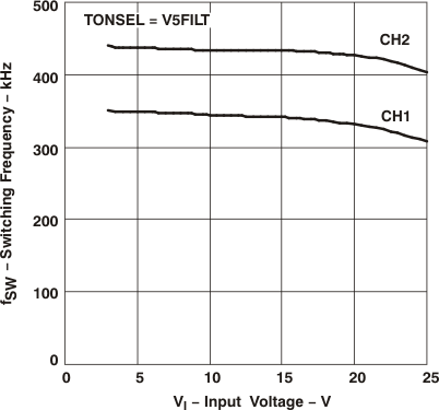
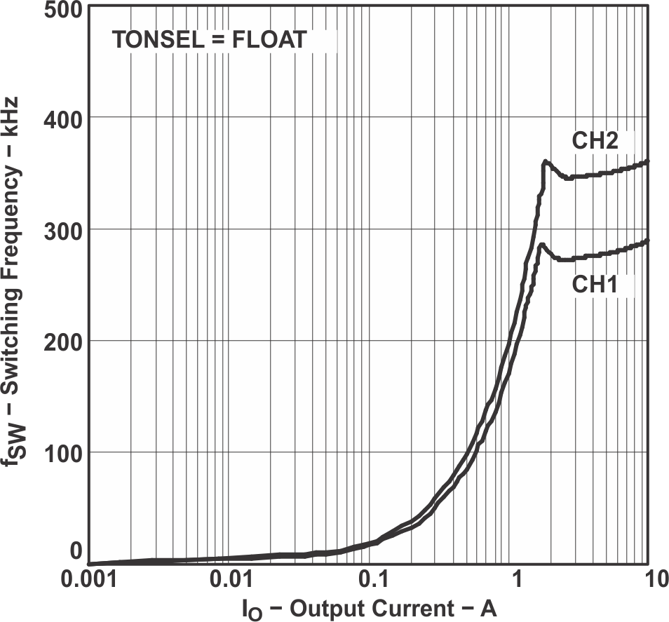
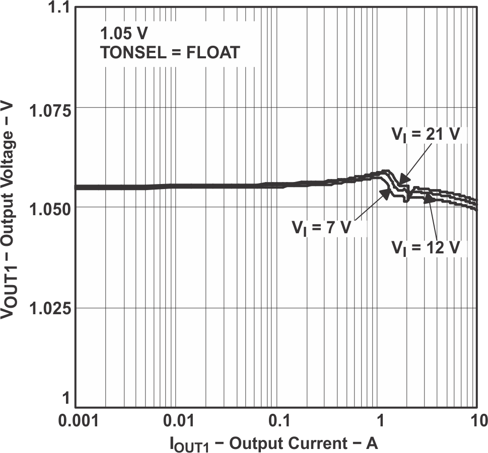
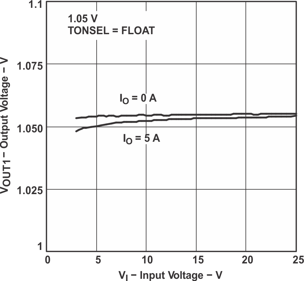
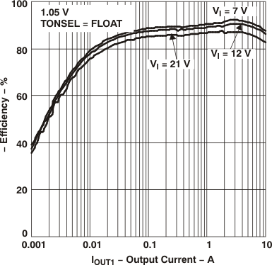
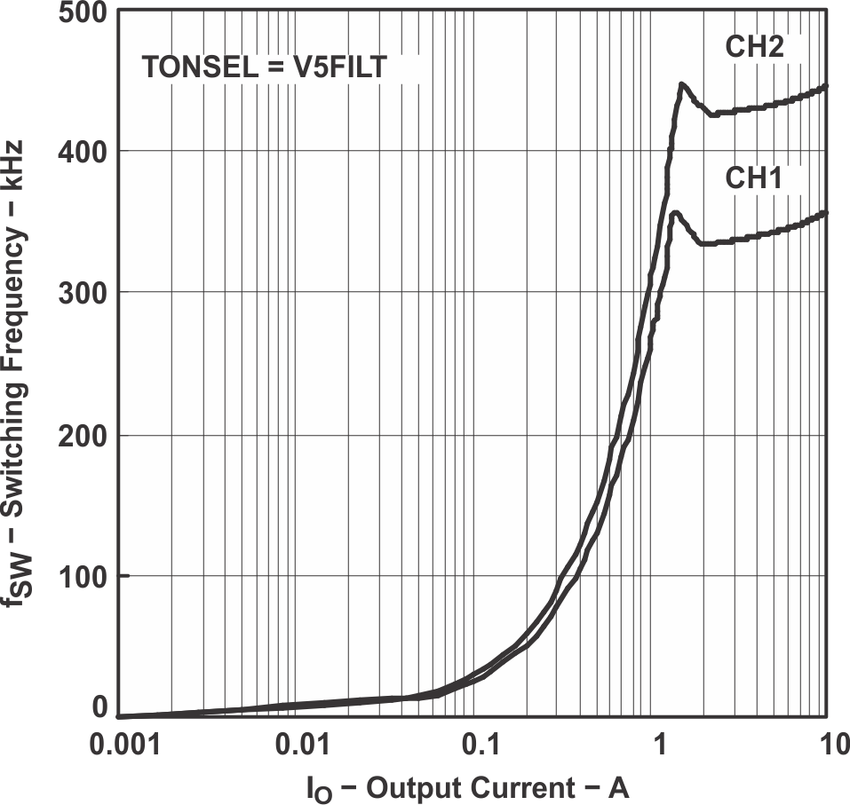
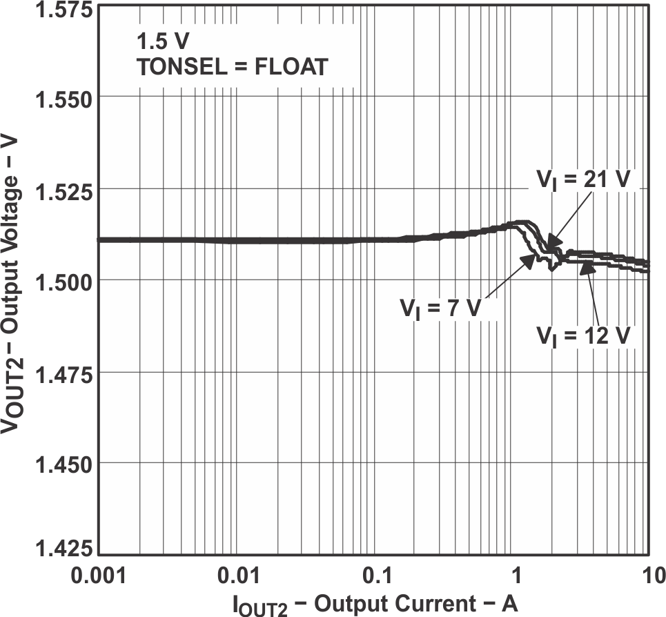
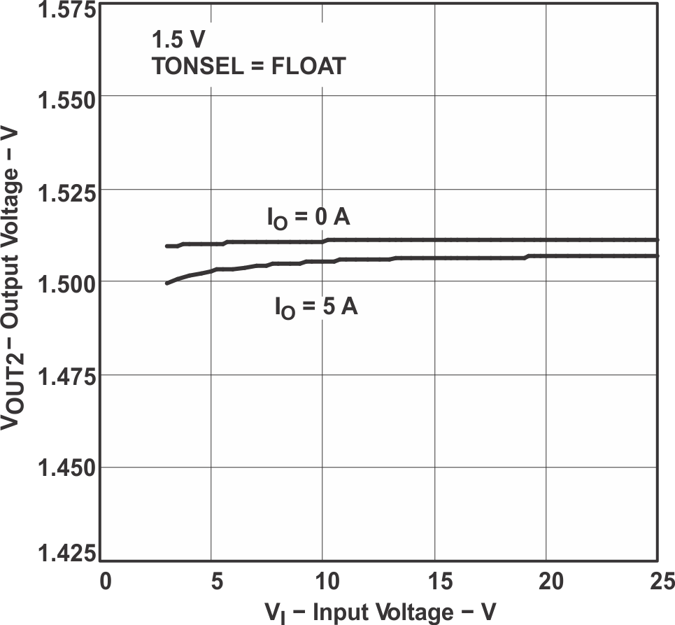
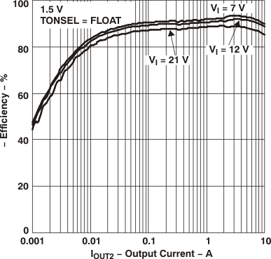
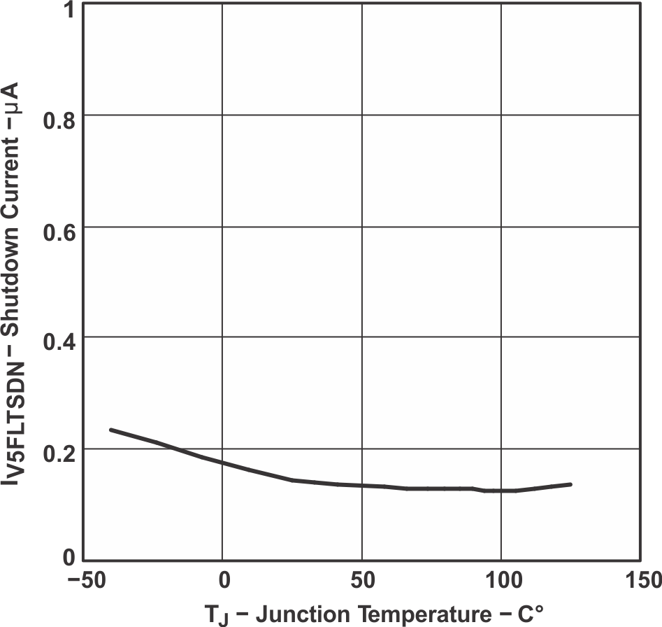
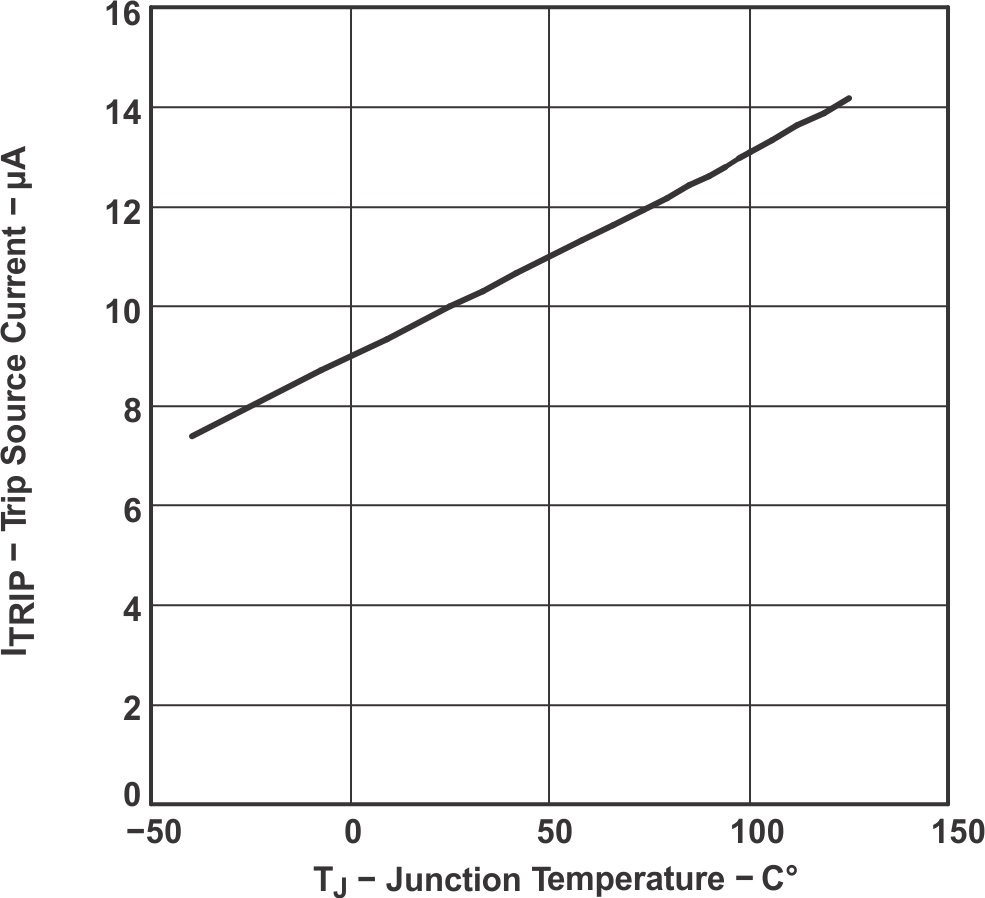
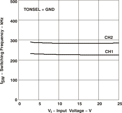
6.5 Typical Characteristics
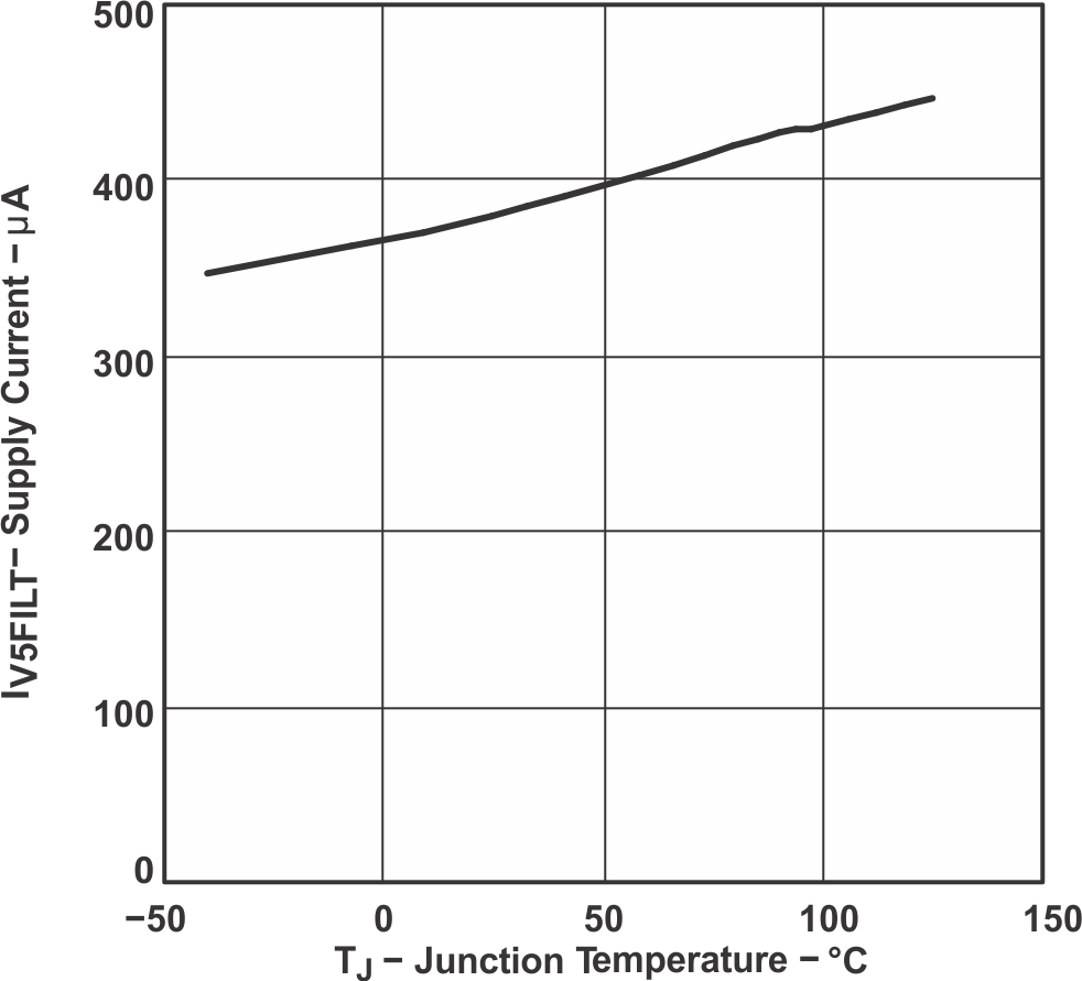
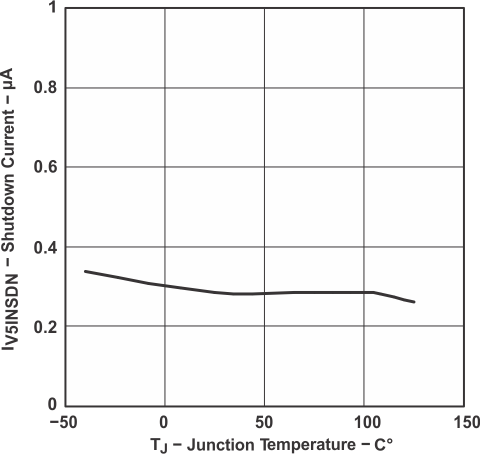
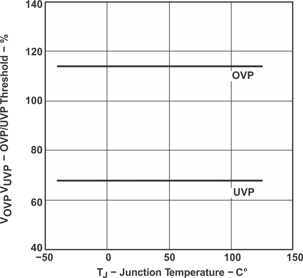
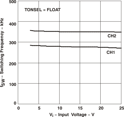
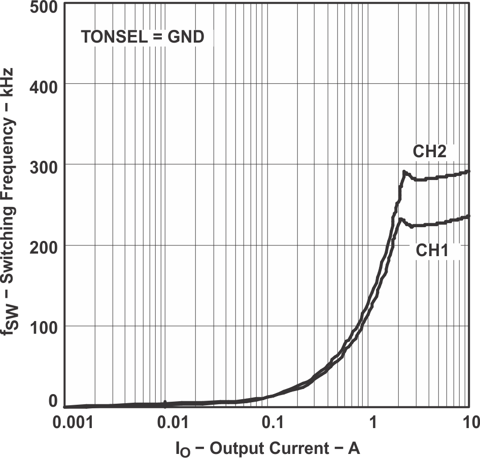
(2) The data of – are measured from the Typical Application Circuit of and .
(3) The data of – are measured from the Typical Application Circuit of and
(4) The data of – are measured from the Typical Application Circuit of and
(1) The data of – are measured from the Typical Application Circuit of and .