SLVS616C November 2005 – December 2014 TPS51124
PRODUCTION DATA.
- 1 Features
- 2 Applications
- 3 Description
- 4 Revision History
- 5 Pin Configuration and Functions
- 6 Specifications
- 7 Detailed Description
- 8 Application and Implementation
- 9 Power Supply Recommendations
- 10Layout
- 11Device and Documentation Support
- 12Mechanical, Packaging, and Orderable Information
封装选项
机械数据 (封装 | 引脚)
- RGE|24
散热焊盘机械数据 (封装 | 引脚)
- RGE|24
订购信息
8 Application and Implementation
NOTE
Information in the following applications sections is not part of the TI component specification, and TI does not warrant its accuracy or completeness. TI’s customers are responsible for determining suitability of components for their purposes. Customers should validate and test their design implementation to confirm system functionality.
8.1 Application Information
The TPS51124 is typically used as a dual-synchronous buck controller, which convert an input voltage ranging from 3V to 28 V, to output voltage ranging 0.76 V to 5.5 V, targeted for notebook I/O and low voltage system bus supply solutions.
8.2 Typical Application
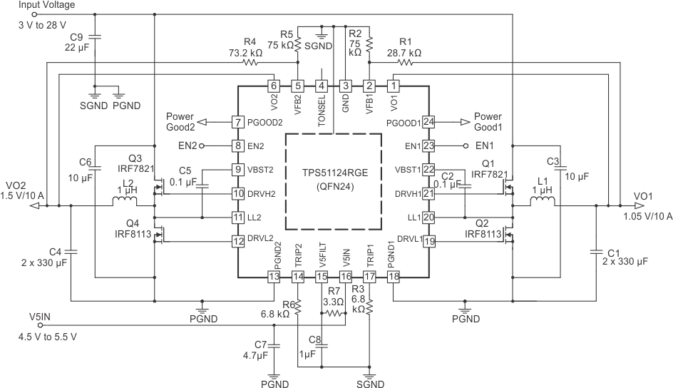
Table 2. Typical Application Circuit Components
| SYMBOL | SPECIFICATION | MANUFACTURER | PART NUMBER |
|---|---|---|---|
| C1 | 330 μF, 2.5 V, 15 mΩ | SANYO | 2R5TPE330MF |
| C4 | 330 μF, 2.5 V, 18 mΩ | SANYO | 2R5TPE330MI |
| L1, L2 | 1 μH, 2 mΩ | TOKO | FDA1254-1R0M |
| C3, C6 | 10 μF, 25 V | TDK | C3225X5R1E106 |
| Q1, Q3 | 30 V, 13 mΩ | International Rectifier | IRF7821 |
| Q2, Q4 | 30 V, 7 mΩ | International Rectifier | IRF8113 |
8.2.1 Design Requirements
Table 3. Design Parameters
| PARAMETER | VALUE | |||
|---|---|---|---|---|
| Input voltage range | 3 V to 28 V | |||
| Channel 1 output voltage | 1.05 V | |||
| Channel 1 output current | 10 A | |||
| Channel 2 output voltage | 1.5 V | |||
| Channel 2 output current | 10 A | |||
8.2.2 Detailed Design Procedure
Figure 19 shows a simplified buck converter system using D-CAP Mode.
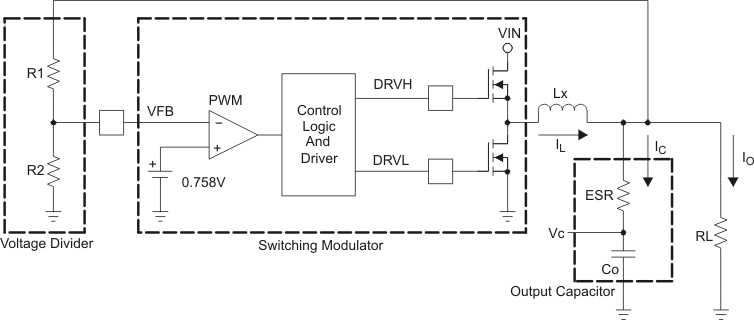
The output voltage is compared with an internal reference voltage after divider resistors, R1 and R2. The PWM comparator determines the timing to turn on the high-side MOSFET. The gain and speed of the comparator is high enough to keep the voltage at the beginning of each on cycle (or the end of off cycle) substantially constant. The DC output voltage may have line regulation due to ripple amplitude that slightly increases as the input voltage increase.
For the loop stability, the 0-dB frequency, f0, defined in Equation 4 needs to be lower than 1/4 of the switching frequency.
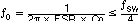
As f0 is determined solely by the output capacitor’s characteristics, loop stability of D-CAP Mode is determined by the capacitor’s chemistry. For example, specialty polymer capacitors (SP-CAP) have Co in the order of several 100 μF and ESR in range of 10 mΩ. These make f0 in the order of 100 kHz or less and the loop is stable. However, ceramic capacitors have f0 at more than 700 kHz, which is not suitable for this operational mode.
Although D-CAP Mode provides many advantages such as ease-of-use, minimum external components configuration, and extremely short response time, a sufficient amount of feedback signal needs to be provided by an external circuit to reduce jitter level. This is due to not employing an error amplifier in the loop. The required signal level is approximately 10 mV at the comparing point (VFB terminal). This gives Vripple at the output node as shown in the following equation.

The output capacitor's ESR should meet this requirement.
The external components selection is much simpler in D-CAP Mode.
- Determine the value of R1 and R2.
- Choose inductor.
- Choose output capacitor(s).
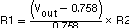
Recommended R2 value is from 10 kΩ to 100 kΩ. Determine R1 using the following equation.
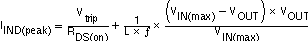
The inductance value should be determined to give the ripple current of approximately 1/4 to 1/2 of maximum output current. Larger ripple current increases the output ripple voltage, improves S/N ratio, and contributes to a stable operation.

The inductor also needs to have low DCR to achieve good efficiency, as well as enough room above peak inductor current before saturation. The peak inductor current can be estimated as follows.
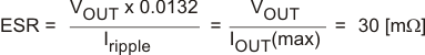
Organic semiconductor capacitor(s) or specialty polymer capacitor(s) are recommended. Determine ESR to meet the required ripple voltage indicated previously. A quick approximation is shown here:
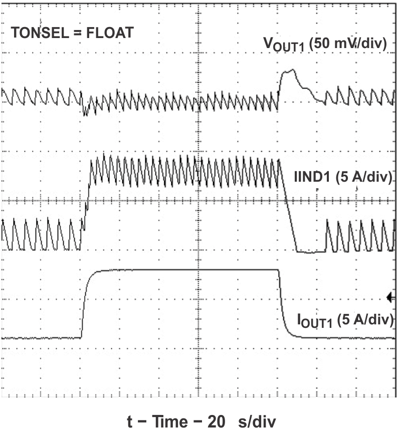
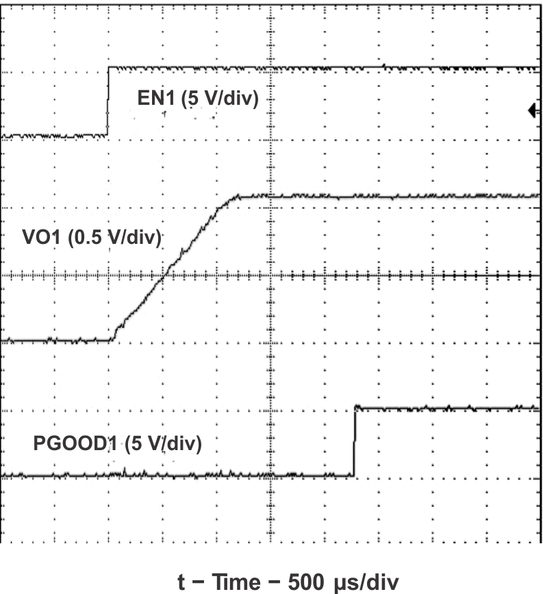
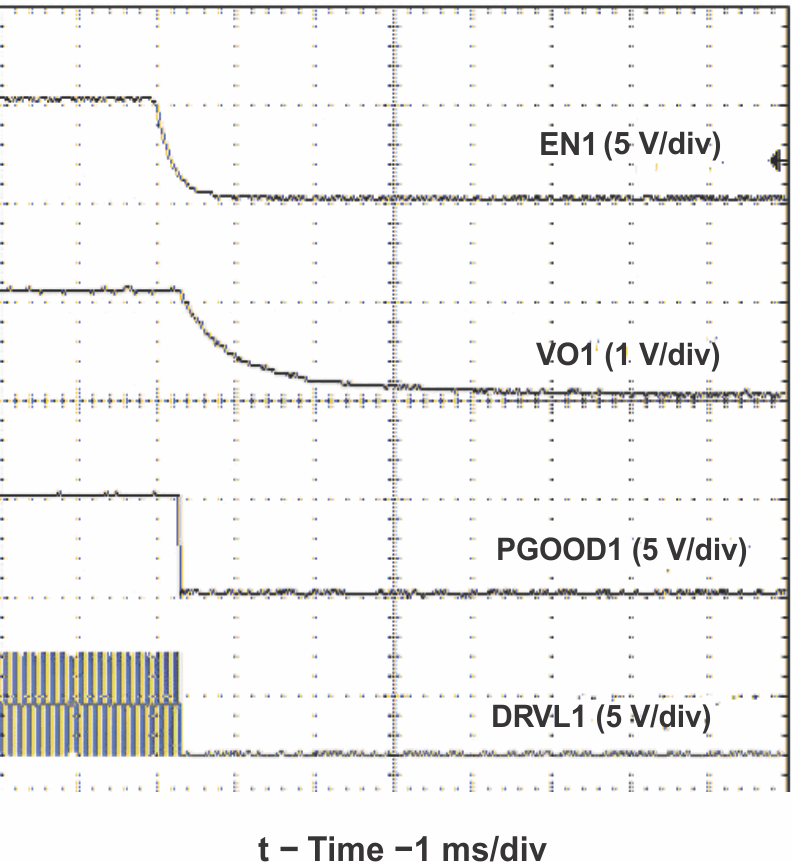
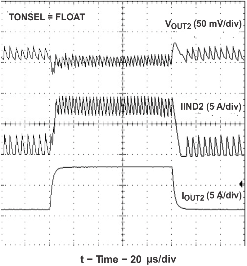
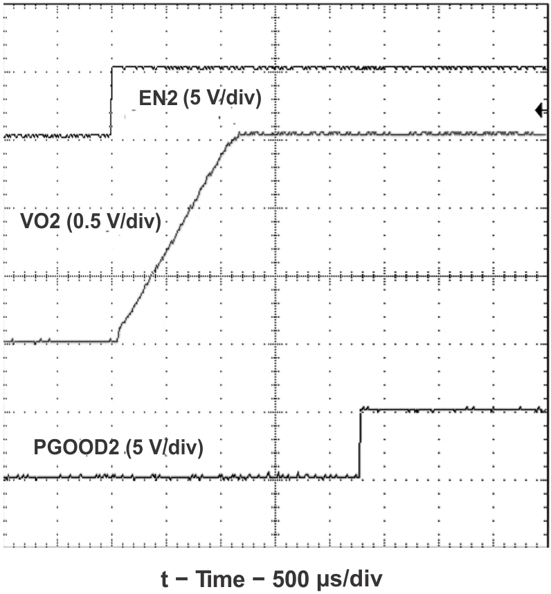
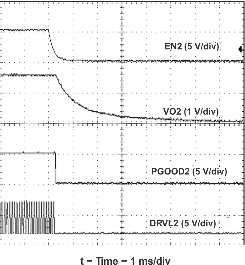
8.2.3 Application Curves