SBVS085J January 2007 – June 2017
PRODUCTION DATA.
- 1 Features
- 2 Applications
- 3 Description
- 4 Revision History
- 5 Device Comparison Table
- 6 Pin Configuration and Functions
- 7 Specifications
- 8 Detailed Description
- 9 Applications and Implementation
- 10Power Supply Recommendations
- 11Layout
- 12Device and Documentation Support
- 13Mechanical, Packaging, and Orderable Information
封装选项
机械数据 (封装 | 引脚)
散热焊盘机械数据 (封装 | 引脚)
- DRV|6
订购信息
9 Applications and Implementation
NOTE
Information in the following applications sections is not part of the TI component specification, and TI does not warrant its accuracy or completeness. TI’s customers are responsible for determining suitability of components for their purposes. Customers should validate and test their design implementation to confirm system functionality.
9.1 Application Information
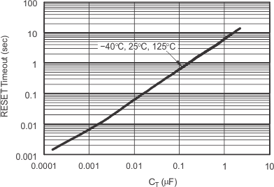
The TPS3808Gxx-Q1 microprocessor supervisory product family is designed to assert a RESET signal when either the SENSE pin voltage drops below VIT or the manual reset (MR) is driven low. The RESET output remains asserted for a user-adjustable time after both the manual reset (MR) and SENSE voltages return above the respective thresholds. A broad range of voltage threshold and reset delay time adjustments are available, allowing these devices to be used in a variety of applications. Reset threshold voltages can be factory-set from 0.82 V to 3.3 V or from 4.4 V to 5 V, while the TPS3808G01-Q1 can be set to any voltage above 0.405 V using an external resistor divider. Two preset delay times are also user-selectable: connecting the CT pin to VDD results in a 300-ms reset delay, while leaving the CT pin open yields a 20-ms reset delay. Additionally, connecting a capacitor between CT and GND allows the designer to select any reset delay period from 1.25 ms to 10 s.
9.2 Typical Application
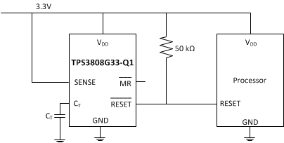
 Figure 14. TPS3808G33-Q1 Typical Application
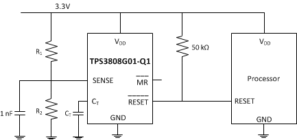
 Figure 15. TPS3808G01-Q1 Typical Application
9.2.1 Design Requirements
The TPS3808Gxx-Q1 device must monitor a 3.3-V input voltage, and drive an active-low reset to the processor when the input voltage drops below the recommended operating voltage of the processor.
9.2.2 Detailed Design Procedure
To monitor the 3.3-V input voltage, TPS3808G33-Q1 is used and the 3.3-V supply is connected directly to the SENSE pin. The open-drain RESET output is connected to VDD through a 50-kΩ resistor. To select the output delay on the RESET pin, connect the CT pin to VDD, left floating, or connect through a capacitor to GND. For more details on selecting this delay, see Selecting the Reset Delay Time.
When using TPS3808G01-Q1, select R1 and R2 resistor values to select the threshold voltage based on the following equation: VIT = (1 + R1 / R2) × 0.405.
9.2.3 Application Curves

