ZHCS840G February   2012  – February 2019 TPS3700

PRODUCTION DATA.  

  1. 特性
  2. 应用
  3. 说明
    1.     Device Images
      1.      简化原理图
      2.      输出与输入阈值和迟滞
  4. 修订历史记录
  5. Pin Configuration and Functions
    1.     Pin Functions
  6. Specifications
    1. 6.1 Absolute Maximum Ratings
    2. 6.2 ESD Ratings
    3. 6.3 Recommended Operating Conditions
    4. 6.4 Thermal Information
    5. 6.5 Electrical Characteristics
    6. 6.6 Timing Requirements
    7. 6.7 Switching Characteristics
    8. 6.8 Typical Characteristics
  7. Detailed Description
    1. 7.1 Overview
    2. 7.2 Functional Block Diagram
    3. 7.3 Feature Description
      1. 7.3.1 Inputs (INA+, INB–)
      2. 7.3.2 Outputs (OUTA, OUTB)
      3. 7.3.3 Window Voltage Detector
      4. 7.3.4 Immunity to Input Terminal Voltage Transients
    4. 7.4 Device Functional Modes
      1. 7.4.1 Normal Operation (VDD > UVLO)
      2. 7.4.2 Undervoltage Lockout (V(POR) < VDD < UVLO)
      3. 7.4.3 Power-On Reset (VDD < V(POR))
  8. Application and Implementation
    1. 8.1 Application Information
      1. 8.1.1 VPULLUP to a Voltage Other Than VDD
      2. 8.1.2 Monitoring VDD
      3. 8.1.3 Monitoring a Voltage Other Than VDD
      4. 8.1.4 Monitoring Overvoltage and Undervoltage for Separate Rails
    2. 8.2 Typical Application
      1. 8.2.1 Design Requirements
      2. 8.2.2 Detailed Design Procedure
        1. 8.2.2.1 Resistor Divider Selection
        2. 8.2.2.2 Pullup Resistor Selection
        3. 8.2.2.3 Input Supply Capacitor
        4. 8.2.2.4 Input Capacitors
      3. 8.2.3 Application Curves
    3. 8.3 Do's and Don'ts
  9. Power-Supply Recommendations
  10. 10Layout
    1. 10.1 Layout Guidelines
    2. 10.2 Layout Example
  11. 11器件和文档支持
    1. 11.1 器件支持
      1. 11.1.1 开发支持
        1. 11.1.1.1 评估模块
      2. 11.1.2 器件命名规则
    2. 11.2 文档支持
      1. 11.2.1 相关文档
    3. 11.3 接收文档更新通知
    4. 11.4 社区资源
    5. 11.5 商标
    6. 11.6 静电放电警告
    7. 11.7 术语表
  12. 12机械、封装和可订购信息

封装选项

请参考 PDF 数据表获取器件具体的封装图。

机械数据 (封装 | 引脚)
  • DSE|6
  • DDC|6
散热焊盘机械数据 (封装 | 引脚)
订购信息

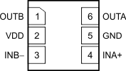
Pin Configuration and Functions

DDC Package
SOT-6
Top View
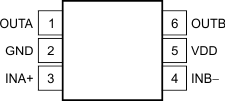
TPS3700 po_bvs187.gif
DSE Package
WSON-6
Top View
TPS3700 po_dse_bvs187.gif

Pin Functions

PIN I/O DESCRIPTION
NAME DDC DSE
GND 2 5 Ground
INA+ 3 4 I This pin is connected to the voltage to be monitored with the use of an external resistor divider. When the voltage at this terminal drops below the threshold voltage (VITP – VHYS), OUTA is driven low.
INB– 4 3 I This pin is connected to the voltage to be monitored with the use of an external resistor divider. When the voltage at this terminal exceeds the threshold voltage (VITP), OUTB is driven low.
OUTA 1 6 O INA+ comparator open-drain output. OUTA is driven low when the voltage at this comparator is below (VITP – VHYS). The output goes high when the sense voltage returns above the respective threshold (VITP).
OUTB 6 1 O INB– comparator open-drain output. OUTB is driven low when the voltage at this comparator exceeds VITP. The output goes high when the sense voltage returns below the respective threshold (VITP – VHYS).
VDD 5 2 I Supply voltage input. Connect a 1.8-V to 18-V supply to VDD to power the device. Good analog design practice is to place a 0.1-µF ceramic capacitor close to this pin.