ZHCSIK0A July   2018  – October 2021 TPS3430

PRODUCTION DATA  

  1. 特性
  2. 应用
  3. 说明
  4. Revision History
  5. Pin Configuration and Functions
  6. Specifications
    1. 6.1 Absolute Maximum Ratings
    2. 6.2 ESD Ratings
    3. 6.3 Recommended Operating Conditions
    4. 6.4 Thermal Information
    5. 6.5 Electrical Characteristics
    6. 6.6 Timing Requirements
    7. 6.7 Timing Diagrams
    8. 6.8 Typical Characteristics
  7. Detailed Description
    1. 7.1 Overview
    2. 7.2 Functional Block Diagrams
    3. 7.3 Feature Description
      1. 7.3.1 CRST
      2. 7.3.2 Window Watchdog
        1. 7.3.2.1 SET0 and SET1
          1. 7.3.2.1.1 Enabling the Window Watchdog
          2. 7.3.2.1.2 Disabling the Watchdog Timer When Using the CRST Capacitor
          3. 7.3.2.1.3 SET0 and SET1 During Normal Watchdog Operation
      3. 7.3.3 Window Watchdog Timer
        1. 7.3.3.1 CWD
        2. 7.3.3.2 WDI Functionality
        3. 7.3.3.3 WDO Functionality
    4. 7.4 Device Functional Modes
      1. 7.4.1 VDD is Below VPOR ( VDD < VPOR)
      2. 7.4.2 VDD is Above VPOR And Below VDD (min)( VPOR < VDD < VDD (min))
      3. 7.4.3 Normal Operation (VDD ≥ VDD (min))
  8. Application and Implementation
    1. 8.1 Application Information
      1. 8.1.1 CRST Delay
        1. 8.1.1.1 Factory-Programmed Watchdog Reset Delay Timing
        2. 8.1.1.2 CRST Programmable Watchdog Reset Delay
      2. 8.1.2 CWD Functionality
        1. 8.1.2.1 Factory-Programmed Timing Options
        2. 8.1.2.2 CWD Adjustable Capacitor Watchdog Timeout
    2. 8.2 Typical Applications
      1. 8.2.1 Monitoring Microcontroller with Watchdog Timer - Design 1
        1. 8.2.1.1 Design Requirements - Design 1
        2. 8.2.1.2 Detailed Design Procedure - Design 1
          1. 8.2.1.2.1 Meeting the Minimum Watchdog Reset Delay - Design 1
          2. 8.2.1.2.2 Setting the Watchdog Window - Design 1
          3. 8.2.1.2.3 Calculating the WDO Pull-up Resistor - Design 1
      2. 8.2.2 Monitoring Microcontroller with a Programmed Window Watchdog Timer - Design 2
        1. 8.2.2.1 Design Requirements - Design 2
        2. 8.2.2.2 Detailed Design Procedure - Design 2
          1. 8.2.2.2.1 Meeting the Minimum Watchdog Reset Delay - Design 2
          2. 8.2.2.2.2 Setting the Watchdog Window - Design 2
          3. 8.2.2.2.3 Calculating the WDO Pull-up Resistor - Design 2
      3. 8.2.3 Monitoring Microcontroller with a Latching Window Watchdog Timer - Design 3
        1. 8.2.3.1 Design Requirements - Design 3
        2. 8.2.3.2 Detailed Design Procedure - Design 3
          1. 8.2.3.2.1 Meeting the Latching Output Requirement - Design 3
          2. 8.2.3.2.2 Setting the Watchdog Window - Design 3
        3. 8.2.3.3 Application Curve - Design 3
  9. Power Supply Recommendations
  10. 10Layout
    1. 10.1 Layout Guidelines
    2. 10.2 Layout Example
  11. 11Device and Documentation Support
    1. 11.1 Device Support
    2. 11.2 Documentation Support
      1. 11.2.1 Related Documentation
    3. 11.3 接收文档更新通知
    4. 11.4 支持资源
    5. 11.5 Trademarks
    6. 11.6 Electrostatic Discharge Caution
    7. 11.7 术语表
  12. 12Mechanical, Packaging, and Orderable Information

封装选项

机械数据 (封装 | 引脚)
散热焊盘机械数据 (封装 | 引脚)
订购信息
Meeting the Minimum Watchdog Reset Delay - Design 2

The TPS3430 features three options for setting the watchdog reset delay: connecting a capacitor to the CRST pin, connecting a pull-up resistor, and leaving the CRST pin unconnected. If the CRST pin is either unconnected or pulled up the minimum timing requirement cannot be met, thus an external capacitor must be connected to the CRST pin. Because a minimum time is required, the worst-case scenario is a supervisor with a high CRST charging current (ICRST) and a low CRST comparator threshold (VCRST). For applications with ambient temperatures ranging from –40°C to +125°C, CCRST can be calculated using ICRST(MAX), VCRST(MIN), and solving for CCRST in Equation 5:

Equation 5. GUID-0DDF6F3C-0A6A-4A32-B26C-898C82E48362-low.gif

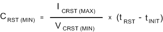
When solving Equation 5, the minimum capacitance required at the CRST pin is 0.086 μF. If standard capacitors with ±10% tolerances are used, then the minimum CRST capacitor required can be found in Equation 6:

Equation 6. GUID-303F28E0-E30E-4EFE-843B-02CB69D901BE-low.gif

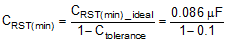
Solving Equation 6 where Ctolerance is 0.1 or 10%, the minimum CCRST capacitor is 0.096 μF. This value is then rounded up to the nearest standard capacitor value, so a 0.1-μF capacitor must be used to achieve this reset delay timing. If voltage and temperature derating are being considered, then also include these values in Ctolerance.